当前位置:网站首页>Memory computing integration: AI chip architecture in the post Moorish Era
Memory computing integration: AI chip architecture in the post Moorish Era
2022-07-04 12:06:00 【Said the shepherdess】
Save and calculate in one , Or in memory calculation , It refers to the calculation centered design in the traditional von Neumann architecture , Change to data storage centric design , That is to use memory to calculate data , So as to avoid data handling “ Storage wall ” and “ Power wall ”, Greatly improve the parallelism and energy efficiency of data . This architecture is especially suitable for those who require a lot of computing power 、 Low power terminal device , Such as wearable equipment 、 Mobile devices 、 Smart home, etc .
1. Limitations of von Neumann architecture
The first is performance .
Under the classic von Neumann architecture , Data storage and calculation are separated , processor CPU Data exchange between memories is carried out through data bus . But due to the internal structure of processor and memory 、 Different process and packaging , There is also a great difference in the performance of the two . from 1980 Year begins , The performance gap between processor and memory is widening , The access speed of memory is far from keeping up CPU Data processing speed , This is a journey between memory and processor “ Storage wall ”, It seriously restricts the overall performance improvement of the chip .

The second is power consumption .
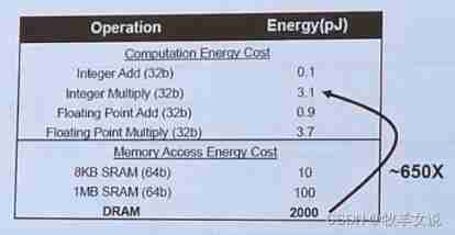
As mentioned earlier , Due to the separation of processor and memory , In the process of processing data , First, you need to move the data from the memory to the processor through the bus , After processing , Then move the data back to the memory for storage . The energy consumption of data in the process of handling is floating-point operation 4~1000 times . With the progress of semiconductor technology , Although the overall power consumption decreases , But the power consumption ratio of data handling is increasing . According to research , stay 7nm Time , The sum of memory access power consumption and communication power consumption accounts for 63% above .
Due to the existence of the above storage wall and power consumption wall , The traditional von Neumann architecture is no longer suitable for big data computing AIoT scene , Therefore, the demand for new computing architecture came into being .
2. Solutions
Design for new computing architecture , Researchers have proposed a variety of solutions , It can be roughly divided into three categories :
(1) High speed bandwidth data communication , Including optical interconnection 、2D/3D The stack .
High speed bandwidth data communication mainly solves the problem of storage wall by improving the communication bandwidth . Optical interconnection technology can realize high-speed data transmission , Reduce power consumption .2.5D/3D Stacking technology is to stack multiple chips together , Increase the communication bandwidth by increasing the parallel width or using serial transmission .
(2) Near memory operation .
The basic approach of near memory computing is to store data as close to the computing unit as possible , Thus, the delay and power consumption of data handling are reduced . at present , The architecture of near memory computing mainly includes multi-level cache architecture and high-density on-chip storage .
(3) Save and calculate in one , That is, the algorithm of the memory itself is embedded .
The core idea of memory computing integration or memory computing is , Through the algorithm embedding of the memory unit itself , So that the calculation can be completed in the memory unit .
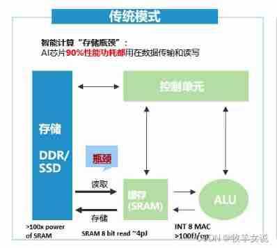
Power consumption comparison
Traditional off chip storage 、 The comparison of power consumption between near memory computing and in memory computing can be seen in the figure below :

picture source : Qing Yuan LIVE The first 28 period | The next generation AI chip — Hard core and soft core of in memory computing _ Bili, Bili _bilibili
3. Memory computing integrated chip features
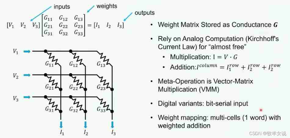
As we mentioned earlier , The core idea of integrating storage and Computing , It is through algorithm embedding in the storage unit itself , say concretely , The main thing is to AI The weight data of the model is stored in the memory unit , Then the core circuit of memory is designed , The process of making data flow is the process of point multiplication of input data and weight in the simulation domain , It is equivalent to realizing weighted accumulation of input , That is, convolution . Because convolution is the core unit of deep learning algorithm , Therefore, the integration of saving and computing is very suitable for deep learning . This architecture completely eliminates the memory access delay , And greatly reduce the power consumption , It is a true fusion of storage and Computing . meanwhile , Because computing is completely coupled to storage , Therefore, finer grained parallelism can be developed , Get higher performance and energy efficiency .
picture source : Qing Yuan LIVE The first 28 period | The next generation AI chip — Hard core and soft core of in memory computing _ Bili, Bili _bilibili
4. Current status of memory computing integrated chip
(1) Technology implementation
Classify according to the volatility during storage , There are two ways to realize the integrated storage and Computing Technology ,
- Based on volatility 、 The existing process is mature SRAM、DRAM Realization ;
- Based on nonvolatile 、 New memory such as phase change memory PCM、 Resistive memory RRAM/ Memristor ReRAM、 Floating gate device or flash memory Flash To achieve .
Volatile memory SRAM and DRAM The technology is mature , It is the main commercial memory product at present . therefore , Many manufacturers and research institutions began to base on SRAM and DRAM Research on in memory computing . However, due to the different manufacturing processes of memory and processor , There is still no good balance between processing performance and storage capacity .
Nonvolatile memory includes spin moment magnetic memory STTRAM、 Phase change memory PCM、 Resistive memory RRAM etc. , The research of these memories has also made rapid development in recent ten years , Increasing capacity , And it has the natural fusion of computing and storage , Researchers also began to consider the possibility of building a memory computing integrated system based on nonvolatile memory . However, the corresponding manufacturers and processes are not yet mature , There is still a certain distance from real business .
(2) Competition pattern
In recent years , A number of start-ups integrating deposit and accounting have emerged at home and abroad .
Foreign well-known savings and accounting integrated start-ups include Mythic、Syntiant. in addition , Veteran giant Samsung is also based on HBM2 DRAM Developed its integrated storage and Computing Technology .
Domestic enterprises are blooming , Including Zhicun Technology ( be based on Flash)、 Flash semiconductor ( Based on memristor PLRAM)、 Xinyi Technology ( be based on RRAM)、 Hengshuo semiconductor ( be based on NOR Flash)、 Rear rub intelligence ( Research directions include SRAM/MRAM/RRAM)、 Jiutianruixin ( be based on SRAM) etc. . in addition , And brother Ali Flathead ( be based on DRAM Of 3D Bonding stack ).
边栏推荐
- (August 10, 2021) web crawler learning - Chinese University ranking directed crawler
- Summary of Shanghai Jiaotong University postgraduate entrance examination module firewall technology
- Take advantage of the world's sleeping gap to improve and surpass yourself -- get up early
- Entitas learning [iv] other common knowledge points
- netstat
- Local MySQL forget password modification method (Windows) [easy to understand]
- Climb Phoenix Mountain on December 19, 2021
- TCP fast retransmission sack mechanism
- Detailed explanation of classic process synchronization problems
- Method of setting default items in C # ComboBox control code
猜你喜欢
What if the chat record is gone? How to restore wechat chat records on Apple Mobile
Enter the smart Park, and change begins here
OSI seven layer reference model
Climb Phoenix Mountain on December 19, 2021
Some summaries of the 21st postgraduate entrance examination 823 of network security major of Shanghai Jiaotong University and ideas on how to prepare for the 22nd postgraduate entrance examination pr

Review of week 278 of leetcode II
2021 annual summary - it seems that I have done everything except studying hard
(2021-08-20) web crawler learning 2

Exness: positive I win, negative you lose
Experiment 7. IPv6
随机推荐
[Yunju entrepreneurial foundation notes] Chapter II entrepreneur test 21
Detailed explanation of classic process synchronization problems
[Yunju entrepreneurial foundation notes] Chapter II entrepreneur test 7
Data communication and network: ch13 Ethernet
Process communication and thread explanation
World document to picture
[Chongqing Guangdong education] National Open University spring 2019 2727 tax basis reference questions
[Yunju entrepreneurial foundation notes] Chapter II entrepreneur test 8
Some tips on learning database
Introduction of network security research direction of Shanghai Jiaotong University
SQL greatest() function instance detailed example
[Yunju entrepreneurial foundation notes] Chapter II entrepreneur test 14
Exceptions and exception handling
Exness: positive I win, negative you lose
QQ get group information
Sys module
2021-11-02
priority_ queue
Application of slice
Force buckle 142 Circular linked list II