当前位置:网站首页>Brushless drive design -- on MOS drive circuit
Brushless drive design -- on MOS drive circuit
2022-07-05 23:20:00 【Xiao Xiang is a der】
MOS drive
Preface
Last weekend, , When debugging the brushless motor drive, it always explodes inexplicably , The mentality is gone , There's really no choice but to CSDN and B Station University relearned relevant theoretical knowledge , The following are my study notes , For reference only , If there are mistakes, you are welcome to criticize and correct .
MOS Actual circuit model
MOS As a common device, I believe everyone is familiar , I won't go into details about its classification and principle , In the model electricity, the teacher will teach us the following schematic diagrams and symbols , The equivalent model with parasitic capacitance is rarely mentioned .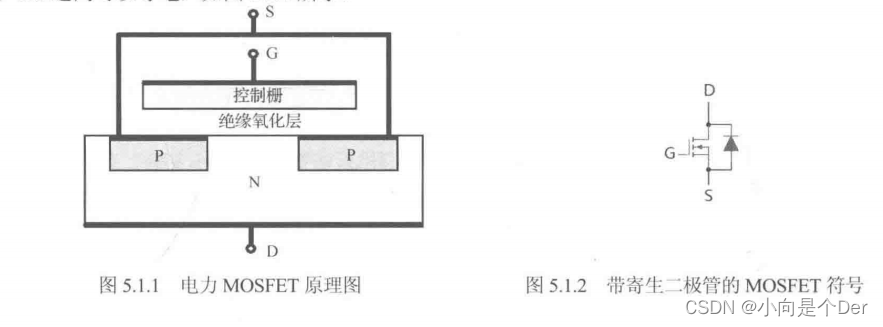
Parasitic capacitance
As shown in the figure below , Actually MOS Devices are not like the ones introduced in books , Due to the manufacturing process 、 Materials and reasons for packaging ,MOS The gate of the device (g) Source pole (s) Drain electrode (d) There will be a parasitic capacitance between the three electrodes , from MOS When it is made, it comes with . These three parasitic capacitors are named :Cgs、Cgd、Cds, The specific value will be indicated in the data manual .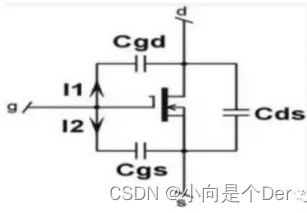
Here we use the commonly used 7843 For example , It is recorded in its data book , Note in the data book , Generally, whether to directly mark the specific value of the above capacitance , Instead, use the input capacitance 、 Output capacitance 、 The reverse conductivity capacitance indicates , The relationship between them is as follows :
Input capacitance (Input Capacitance)Ciss=Cgd+Cgs
Output capacitance (Output Capacitance) CDSS=Cgd+Cds
Reverse conduction capacitance ( Reverse Transfer Capacitance) Crss=Cgd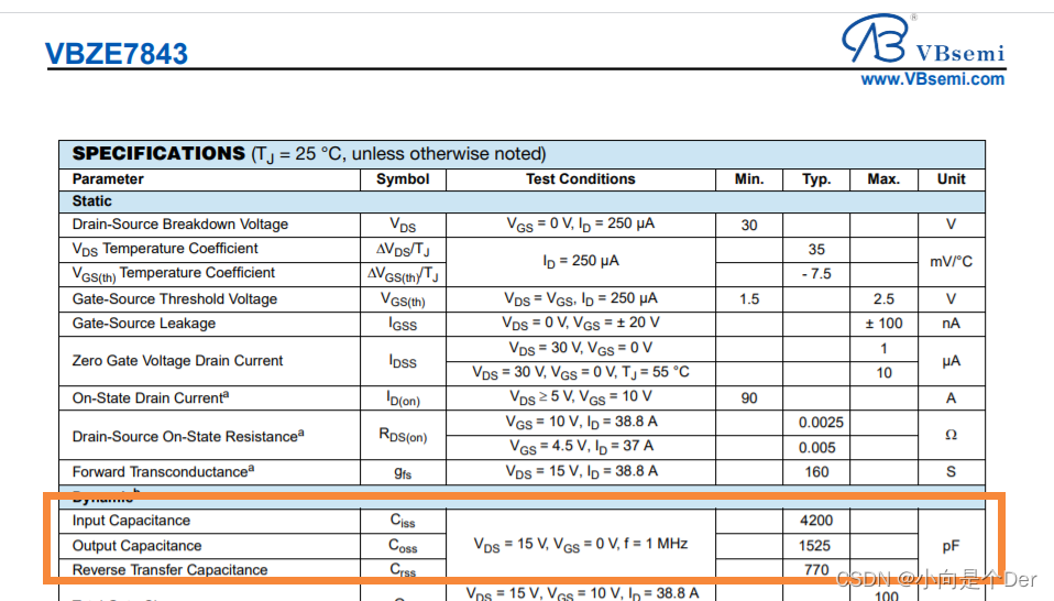
According to the above formula, you can get this 7843 Of Cgs=4200-770=3430pf, About equal to 3.5nf.
Parasitic inductance
In order to better understand the following simulation process , Here is another point that needs to be added , That is parasitic inductance , For its introduction, please refer to this article : How does parasitic inductance come into being _ What is the cause of parasitic inductance .
Simulation
After knowing the parasitic inductance and capacitance , You can start the simulation , This is just to illustrate the phenomenon , Qualitative analysis , So the parameter setting is not very rigorous . Here, the parasitic inductance selected by the author is 100nH, The value of parasitic capacitance is 3.5nF,MOS choose NMOS, The control signal is 1KHZ, Duty ratio 10% Of PWM wave form .
Simulation 1 The grid is connected in series with a small resistor
This simulation aims to illustrate MOS The controlled grid is connected in series with a small resistor R2 The role of , According to the previous analysis , We know , In practice MOS There are parasitic inductance and capacitance in the circuit , After equivalence, the simulation circuit shown in the figure below can be obtained .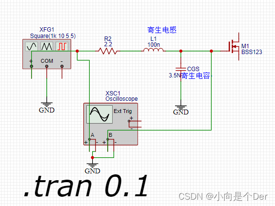
You can find , After adding the grid resistance, a RLC circuit , According to Kirchhoff's law , stay 0 The following transfer function can be obtained by Laplace transformation under the initial conditions .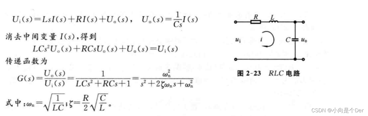
among ωn Is the undamped natural oscillation angular frequency ;ζ It's system resistance , According to the transfer function , Because the circuit is fixed , Components are also fixed , therefore ωn Is constant ,ζ It can increase with the increase of resistance . In the description of typical second-order system by automatic control principle ,ζ In different ranges , The system output will have different states :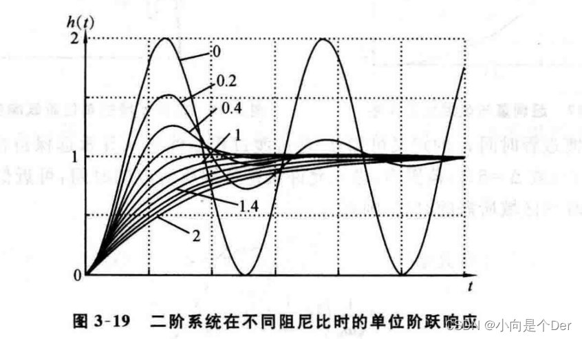
0<ζ<1: Underdamped state 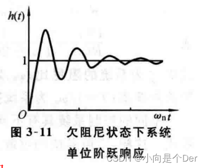
ζ=1: Critical damping state 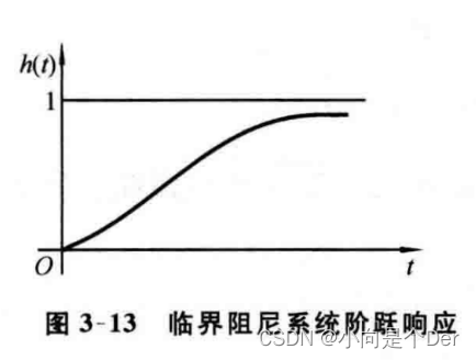
ζ>1: Overdamped state 
The optimum damping ratio is ζ=0.707.
When R2=2.2Ω, When diodes are not paralleled in reverse
The actual waveform of the grid drive is as follows :
here ζ=0.021, It belongs to underdamped state , The overshoot is about 50%, The adjustment time is about 580ns, There is a ringing phenomenon .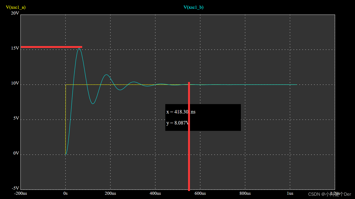
It can be found that there will be overshoot on the rising edge , And the overshoot is very large , If , The pressure resistance value of the pipe is not enough , It is likely to be damaged due to this overshoot .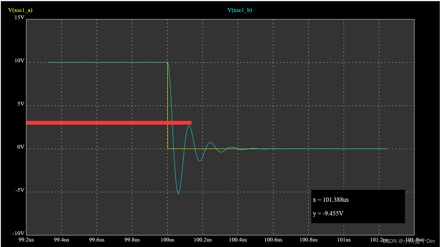
Again , The falling edge position also has overshoot , If the overshoot is too large , Reached MOS On voltage of , It is likely to make MOS Misleading communication occurs at the time when it should be closed , This is for use. MOS Composed of H Bridge and three-phase bridge circuit is fatal , If the misleading pass time exceeds the set dead time , There will be a time when the upper bridge arm and the lower bridge arm are connected at the same time , It is equivalent to directly shorting the positive and negative power supply of the power part , An instant of current is enough to light up your MOS tube .
So in order to protect the circuit safety , We must reduce overshoot as much as possible , Eliminate the ringing phenomenon of grid drive .
When R2=4.7Ω, When diodes are not paralleled in reverse
The actual waveform of the grid drive is as follows :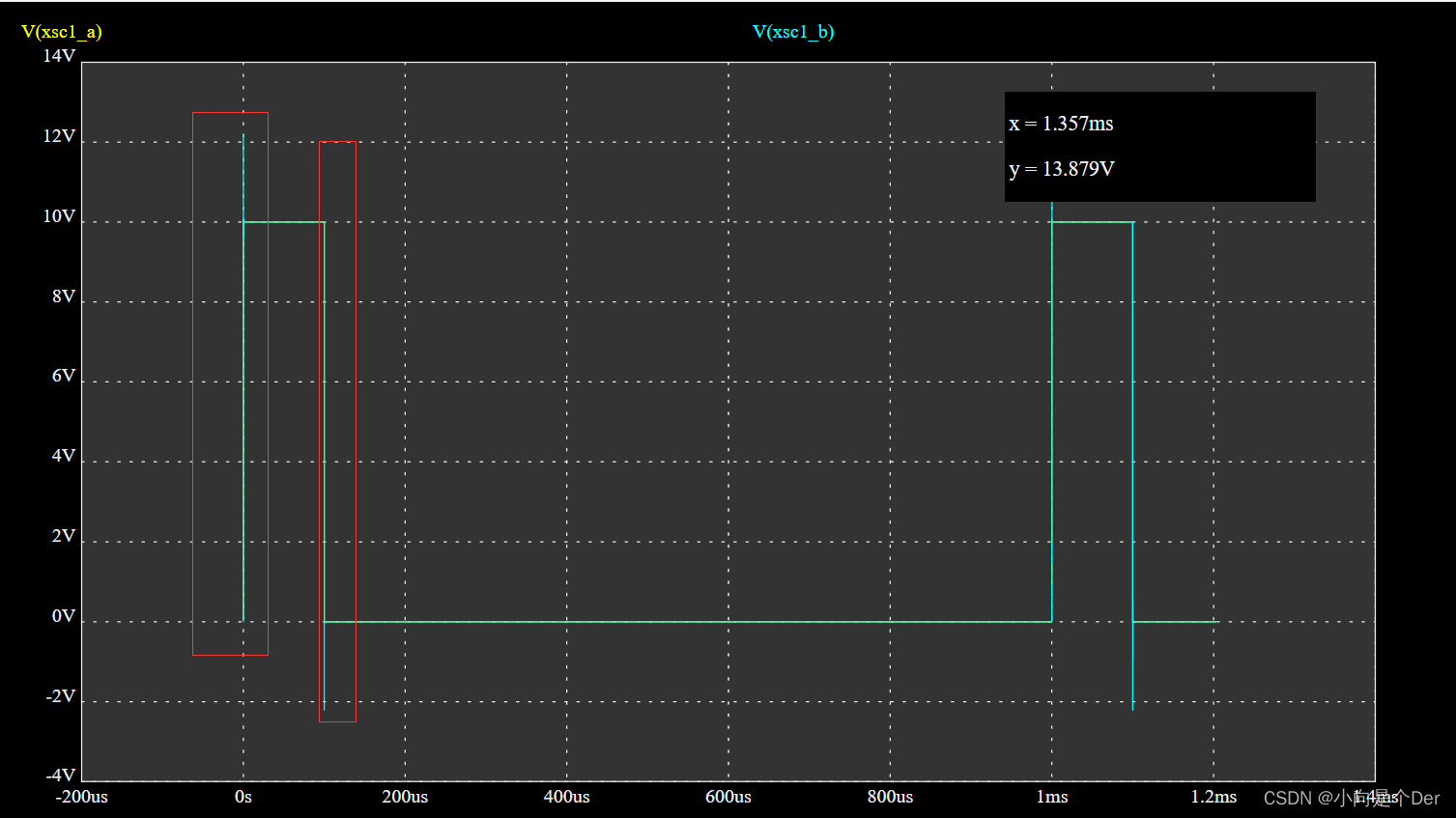
here ζ=0.4396, It is still under damped , The overshoot is about 21%, The adjustment time is about 370ns.
Rising edge :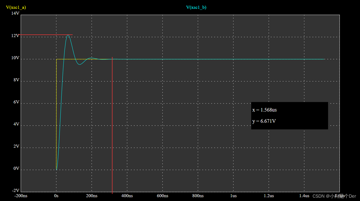
Falling edge :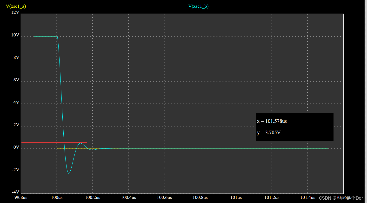
When R2=7.56Ω, When diodes are not paralleled in reverse
here ζ=0.707, It is the best damping ratio in the automatic control principle , Here is just a simple demonstration of the state of the system output at the best damping ratio , It should be emphasized that this value is not the best value in the actual system .
At this time, the overshoot of the rising edge is 5%, Adjustment time ts=180ns.
When R2=10.7Ω, When diodes are not paralleled in reverse
The actual waveform of the grid drive is as follows :
here ζ=1, It still belongs to the critical damping state , The overshoot disappeared , The ring also disappeared , The adjustment time is about 153ns.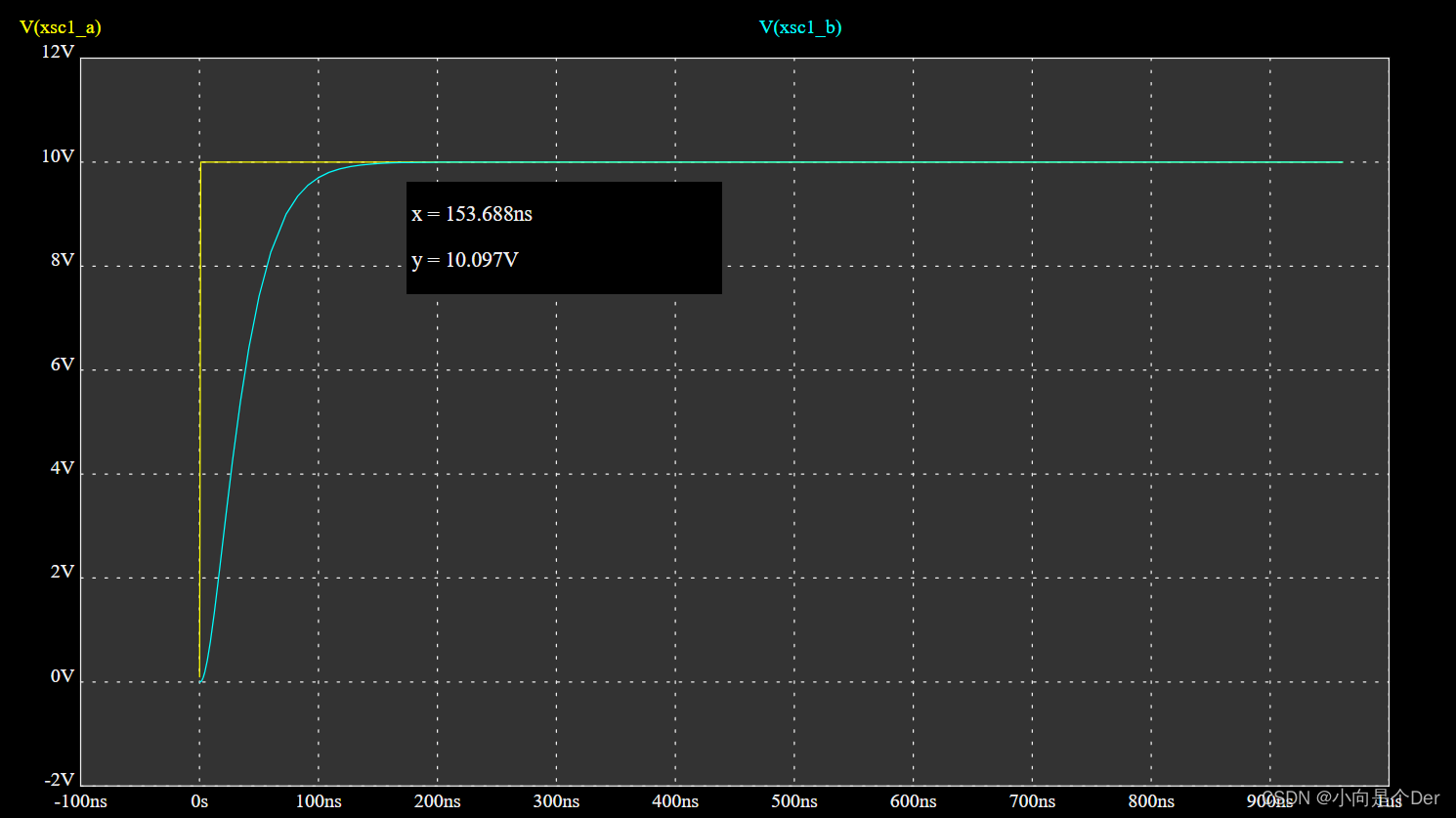
Falling edge waveform :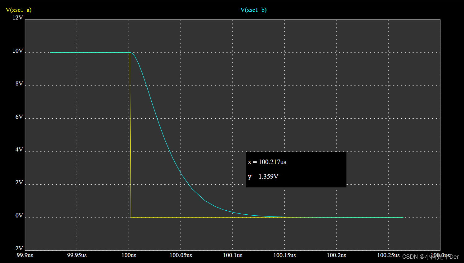
It can be found that the resistance value at this time has met our expectations , No ring , There is no overshoot , Then continue to increase the resistance , Make the system become over damped , What will happen ?
When R2=15Ω, When diodes are not paralleled in reverse
ζ=1.403, It can be found that the system still has no overshoot and ringing , But adjust the time ts Also added , This is for our MOS It's not good for control , The longer the rise time ,MOS The longer it is in the half open and half closed state ,MOS Fever will be more serious , You can check the video for specific explanations :
【 Give Way MOS It's worth burning Ring the bell , Explanation of stray inductance - Bili, Bili 】
【 There is no formula MOS Popular explanation of Miller capacitor - Bili, Bili 】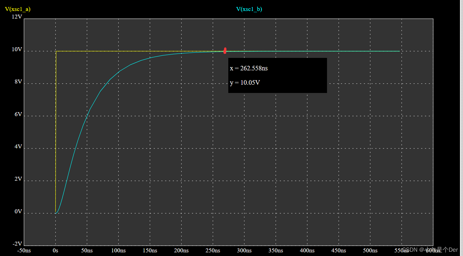
Simulation 2 The grid is connected in series with a small resistor + Anti parallel diode
In the gate drive circuit , In addition to the resistance mentioned above R2 Outside , Many schemes will add an anti parallel diode , So what is the role of adding this diode ?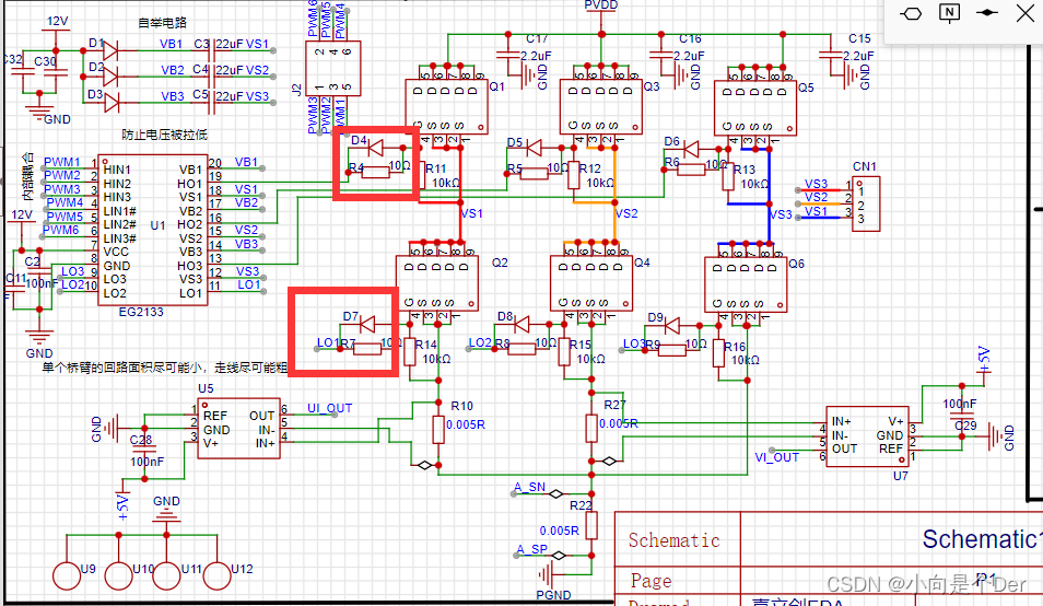
The simulation circuit is as follows :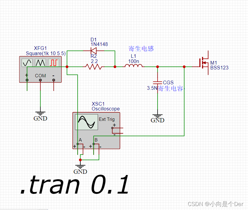
When R2=10.7, When connecting diodes in parallel
The actual waveform of the grid drive is as follows :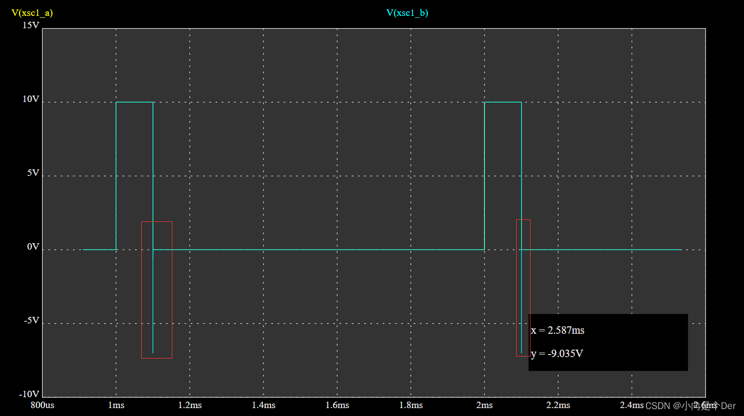
Rising edge ( Parallel diode ):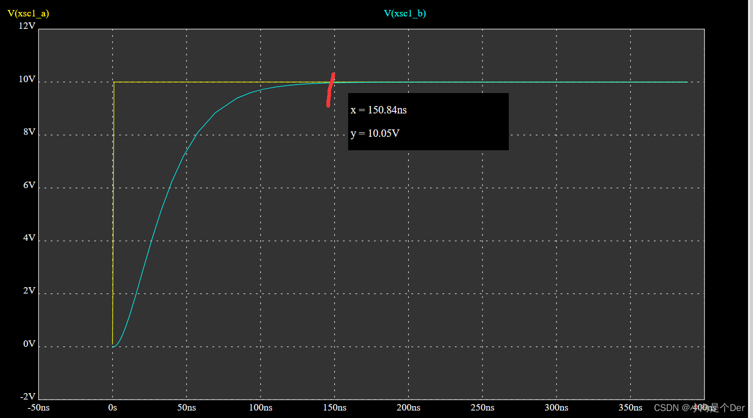
Rising edge ( Diodes not connected in parallel ):
It can be found that adding diodes has no effect on the rising edge .
Falling edge waveform ( Parallel diode ):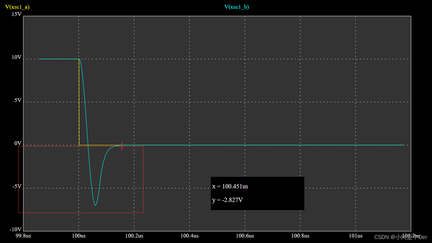
Falling edge waveform ( Diodes not connected in parallel ):
Observe the falling edge , You can find , Compared with the circuit without parallel diodes , A reverse voltage appears on the falling edge , This is good for MOS Quickly turn off , Can further protect MOS.
Other options
In addition to the above processing method, the gate can also be added RC Circuit to eliminate ringing and overshoot , Refer to this video for specific explanation .【LC Classic application of series resonance _mos Why should a small resistor be added to the tube drive circuit ?- Bili, Bili 】
MOS Tube and its peripheral circuit design .
summary
of MOS The introduction of grid drive is recorded here , If there is anything inappropriate in the article, you are welcome to criticize and point out .
reference
Introduction to analog electronic design Yang Yan Fu Qiang
Automatic control principle Wu Huaiyu
边栏推荐
- UVA11294-Wedding(2-SAT)
- Selenium+Pytest自动化测试框架实战
- 透彻理解JVM类加载子系统
- Scala concurrent programming (II) akka
- grafana工具界面显示报错influxDB Error
- How to design API return code (error code)?
- Composition of interface
- 基于脉冲神经网络的物体检测
- Object detection based on impulse neural network
- Sum of two numbers, sum of three numbers (sort + double pointer)
猜你喜欢
并查集实践
![[original] what is the core of programmer team management?](/img/11/d4b9929e8aadcaee019f656cb3b9fb.png)
[original] what is the core of programmer team management?

视频标准二三事

Using LNMP to build WordPress sites
Week 17 homework
基于脉冲神经网络的物体检测
One article deals with the microstructure and instructions of class
PLC编程基础之数据类型、变量声明、全局变量和I/O映射(CODESYS篇 )

Mathematical formula screenshot recognition artifact mathpix unlimited use tutorial
2:第一章:认识JVM规范1:JVM简介;
随机推荐
golang代码检查工具
VS2010编写动态链接库DLL和单元测试,转让DLL测试的正确性
两数之和、三数之和(排序+双指针)
ORB_ SLAM2/3
Leetcode buys and sells stocks
判断二叉树是否为完全二叉树
TVS管和ESD管的技术指标和选型指南-嘉立创推荐
C Primer Plus Chapter 9 question 9 POW function
2022 G3 boiler water treatment simulation examination and G3 boiler water treatment simulation examination question bank
Hainan Nuanshen tea recruits warmhearted people: recruitment of the product experience recommender of Nuanshen multi bubble honey orchid single cluster
数学公式截图识别神器Mathpix无限使用教程
3D reconstruction of point cloud
openresty ngx_lua正则表达式
(4) UART application design and simulation verification 2 - TX module design (stateless machine)
White hat talks about web security after reading 2
asp.net弹出层实例
Basic knowledge of database (interview)
Judge whether the binary tree is a complete binary tree
C Primer Plus Chapter 9 question 10 binary conversion
Use of grpc interceptor