当前位置:网站首页>Basic knowledge 3 - standard unit library
Basic knowledge 3 - standard unit library
2022-07-01 01:27:00 【ty_ xiumud】
review
Synopsys_ Process library format is the de facto library standard . The basic understanding of library format and delay calculation method is the key to successful synthesis Synopsys Process libraries can be divided into two categories :
Logical library : Contain information related only to the integrated process and pass DC For design synthesis and optimization . Such as pin To pin The temporal 、 area 、 Pin type, etc
Physics library : Contains the physical characteristics of the unit , Such as physical size 、 Layer information 、 Unit orientation, etc .
Semiconductor manufacturers provide us DC Compatible process technology library —— Comprehensive library For logical synthesis . Most of the time , Semiconductor manufacturers provide information in binary format .db file , It is also possible to provide only text (ASCII) Format .lib file , Or both .DC The comprehensive library used must be .db Format library . therefore , If we only .lib file , Need to use Library Compiler Convert it to .db file .
The structure of the comprehensive library is shown in the figure below .
It can be divided into two parts , Title part and unit description part . We use smic180 Under process typical.lib Analyze .
The title part mainly introduces the delay model used , Craft corner , Some public parts such as the name of the library , The following part is the description of the curry unit , It is also the main part of this document . There are a total of 214835 That's ok , The first part consists of 250 Describe on the left and right of the line , The rest is a description of the unit .
The corresponding text description is as follows . The following will also summarize the learning by introducing the title part and specific unit descriptions . Reference smic180-typical.lib. The contents of different libraries may be different , But it's all the same .
Library Properties section
- Library Group (library group)
- General properties of process library (general attributes)
- Library documentation (documentation attributes)
- Unit definition (unit attributes)
1, Library Group (library Group)
The library group instruction defines the name of the process library . This instruction must be the first executable line in the library file . for example :
library(my_library)
{
…}
2, General properties of process library (general attributes)
Include the following properties
/* general attributes */
delay_model : table_lookup;
in_place_swap_mode : match_footprint;
library_features(report_delay_calculation); Kurt's characteristics   That is to say, this library has the characteristic of delayed computation

in_place_swap_mode : [match_footpoint/no_swapping];    Alternative exchange   This is the way of matching encapsulation . For specific information, you can refer to other treatments or ask semiconductor manufacturers .
bus_naming_style : "Bus***...";    Bus naming   for example :bus_naming_style:"Bus%spin%d"; This library does not name bus rules .
1)technology Process type
The process attribute definition is used to distinguish which type of design is based on timing analysis . At present, there are two types of designs that require timing analysis , One is ASIC Design , One is FPGA Design . But they are very different in the design process , Therefore, there are differences in time series analysis . Therefore, there are two set values for the process attribute :CMOS and FPGA.
The process attribute identifies the process type used in the library :CMOS( Default )、 FPGA. Process type must be defined first , At the top of the attribute list . If there are no technical attributes in the library ,Library Compiler Default to cmos.
2)in_place_swap_mode
Design tools need to optimize the timing and power consumption of the design , The most basic method is to replace the inappropriate unit with the appropriate unit . However, whether the design tool can be allowed to optimize the unit replacement , It is necessary to define the replacement attribute through unit optimization in the timing information file . Therefore, there are two settings for the cell optimization replacement attribute :match footprint and no swapping.
3)library_features
Process library feature attribute definition Synopsys The tool can be designed by using the command with the feature definition of the process library . The characteristic attributes of the process library are 5 A set value can be selected :report_delay_calculation、report_power_calculation、report_noise_calculation、report_user_data and allow_update_attribute.
4)delay_model Delay model
Indicate the model used to calculate the delay , There are mainly generic_cmos( The default value is )、table-lookup( Nonlinear models )、piecewise-cmos(optional)、dcm(Delay Calculation Module)、polynomial. If the delay model attribute is not defined in the library group , Then the default setting is generic_cmos.
a) Nonlinear models
Most cell libraries include tabular models (table model), It is used to specify delay and check timing for various timing arcs of the unit . These tabular models are called NLDM(Non-Linear Delay Model), Available for delay 、 Output swing calculation or other timing check . The tabular model provides : Delay through the unit under various combinations of input transition time at the unit input pin and output load capacitance at the output pin .
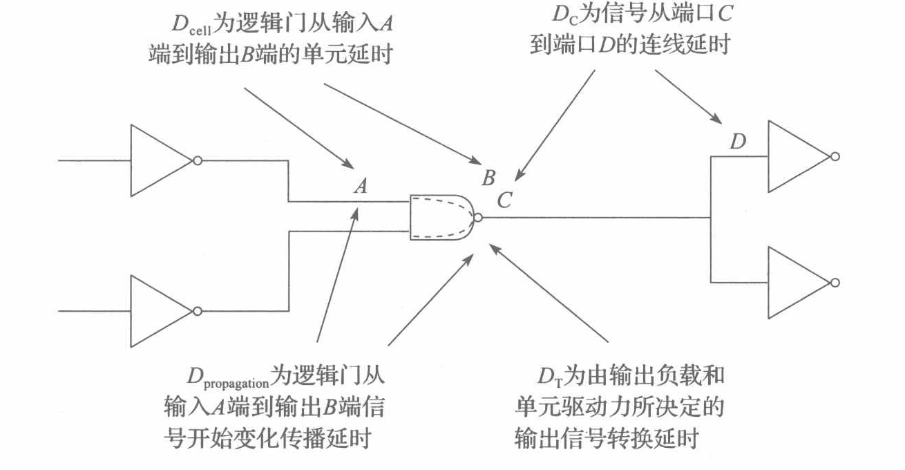
CMOS Nonlinear delay calculation model (NLDM) It is a delay calculation model with high accuracy of time series calculation . stay Synopsys In the process library model , At present, the industry mainly uses the nonlinear delay calculation model . The delay model consists of Input signal conversion time And Output load As index , In time series analysis, the delay is calculated in the form of a two-dimensional look-up table , The actual composition of time series data in the lookup table is shown in the figure below .
Based on the nonlinear time delay calculation model, the usual calculation process is : The delay of a sampling point of the index parameter in the lookup table can be obtained by directly looking up the table , Then the delay is calculated by interpolation algorithm . The accuracy that can be achieved through the nonlinear delay calculation model depends on the rationality of the selection of sampling points and the interpolation algorithm used . As long as the sampling point is reasonable , Better delay results can be obtained by using general polynomial interpolation algorithm . The general interpolation calculation method of delay is shown in the figure

In three-dimensional coordinates ,X Is the jump time of the input port signal Transition time(ns),y Is the load capacitance value of the output terminal Cload(pf),Z Is the delay value Tdelay(ns), The formula is Z=A+B·X+C·Y+D·X·Y If you want to calculate X=0.32、Y=0.05 At the time of the Z value , Just take the closest X、Y Of 4 A sampling point . Construct the following equation

A=0.2006,B=0.1983,C=0.2399,D=0.0677. Into the X、Y that will do

The element delay has been calculated by look-up table and interpolation .
Dc It's through WLM(wire load model) as well as type_tree To calculate , See the following two delay lines to get these two parts .

As shown in the figure below , Computational logic gate U1 Of Dcell When the value of , First determine the conversion time of the input port ,U1 The conversion time of the input port is determined by the previous unit U0 The output of determines . When U0 The output of is rising (rise) When changing time , because U1 The sequence arc of is the reverse sequence arc , therefore U1 The logic gate delay should be in the corresponding U1 Interpolation calculation is performed in the descent sequence arc look-up table . The timing table is a two-dimensional look-up table , Therefore, it is necessary to determine U1 Output load value , Through the interconnect load model and the driving node load value, the total load value at the output end . Last , according to U1 The input port conversion time and the output load capacitance value are used as indexes , In the corresponding U1 The corresponding data can be obtained from the two-dimensional look-up table of descending time series arc , The time delay is directly obtained by interpolation calculation .

3, Library documentation (documentation attributes)
Mainly the version of the library 、 The date of the library 、 And notes .
 revision : ***;
 date : ***;
 comment : ***;
4, Unit definition (unit attributes)
Design Compiler The tool itself has no unit . However, when building process library and producing reports , There has to be a unit . In the library 6 A library level attribute definition unit :
 time_unit : "1ns";    Time unit
 voltage_unit : "1V";    Voltage unit
 current_unit : "1mA";    Unit of current
 pulling_resistance_unit : "1kohm";    Pull up resistance unit
 leakage_power_unit : "1pW";   Leakage power consumption
 capacitive_load_unit : (1.0,pf);   Capacitance unit
The units of values in the unit description are specified in the library , You can use Liberty The command set declares units in the library file .
Environmental Properties section
- Operating environment (operation conditions)
- Threshold definition (threshold definitions)
- Default environment properties (default attributes)
- Templates (templates)
- Scaling factor (k-factors)
- I/Opad attribute (pad attributes)
- Line load model (wire-loads)
1, Working conditions (operation conditions)
The process is specified 、 temperature 、 Voltage and RC Tree model , Synthesis and timing analysis for design .

Here is the basic situation of the library . Will be with slow.lib The content is different . Mainly for temperature 、 Operating environment, voltage, etc .

The working conditions here are the same as we know before PVT The environment is connected .
1)tree_type
tree type Property defines the environment interconnection model used ,DC This attribute value is used to select the appropriate formula when calculating the interconnection delay .
For pre layout estimation , The following three different forms can be used to represent interconnection RC Trees . Please note that , Total length of each interconnect ( And estimates of resistance and capacitance ) In these three cases, it is the same .

Best-case tree: In the best case tree , Assume that the load pin is physically adjacent to the drive pin . therefore , There is no interconnect resistance in the path to the load pin , All interconnect capacitors and pin capacitors from other fan out pins are still used as loads on the drive pins .
Balanced tree: under these circumstances , Assume that each load pin is on a part of the interconnect , And the total resistance and capacitance on each path to the load pin are equal .
Worst-case tree : In the worst case tree , Assume that all load pins are concentrated at the other end of the interconnect . therefore , Each path to the load pin will have all the interconnect resistance and capacitance .
2, Threshold definition (threshold definitions)
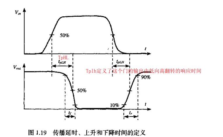
Swing value (slew) Based on the measurement threshold points specified in the library , Most previous generation libraries (0.25um Or older Libraries ) All use 10% and 90% As a pendulum ( Or transition time ) Measurement threshold point .
The selection of swing threshold point corresponds to the linear part of the waveform . With the development of technology , The most linear part of the actual waveform is usually 30% to 70% Between . therefore , Most of the new generation time series libraries specify the swing measurement threshold point as Vdd Of 30% and 70%. however , Because the previously measured transition time is 10% to 90% Between , So when filling the library , Usually the measured 30% to 70% Double the transition time , This is due to Runout derating factor (slew derate factor) Appoint , Usually specified as 0.5. The threshold point of pendulum measurement is 30% and 70% And the runout derating coefficient is 0.5, The equivalent measurement threshold point is 10% and 90%. An example of threshold setting is as follows :
  slew_lower_threshold_pct_fall : 30.0;
  slew_upper_threshold_pct_fall : 70.0;
  slew_lower_threshold_pct_rise : 30.0;
  slew_upper_threshold_pct_rise : 70.0;
  input_threshold_pct_fall      : 50.0; Enter rise / Falling edge sampling point
  input_threshold_pct_rise      : 50.0;
  output_threshold_pct_fall     : 50.0; The output rises / Falling edge sampling point
  output_threshold_pct_rise     : 50.0;
  slew_derate_from_library      : 0.5;

The above setting specifies that the transition time in the table is multiplied by 0.5, In order to obtain the threshold value (30%-70%) Set the corresponding transition time . This means that the values in the table ( And the corresponding index value ) It's actually 10%-90% The measured value of the threshold point . When calibrating the transition time value , First, in the 30%-70% Measure at , Then extrapolate the measured value to 10% to 90%((70-30)/(90-10)= 0.5).
Not specified slew_derate_from_library( The default value is 1.0), This means that the transition time in the library will not be derated (derate)
3, Default environment properties (default attributes)
  /* default attributes */
  default_leakage_power_density	: 0.0;
  default_cell_leakage_power	: 0.0;
  default_fanout_load	: 1.0;
  default_output_pin_cap	: 0.0;
  default_inout_pin_cap	: 0.0035;
  default_input_pin_cap	: 0.0035;
  default_max_transition	: 3.0;
1) Leakage power (leakage_power)
Most standard units are designed to consume power only when the output or state changes . When the unit is energized but there is no behavior , All power consumption is due to leakage current (leakage current). The leak may be due to MOS Caused by subthreshold current of the device , It may also be caused by the tunneling current through the gate oxide . In the past CMOS In process technology , The leakage power is negligible , And it is not the main consideration in the design process . however , With the development of technology , The leakage power becomes larger and larger , Compared with active power , The leakage power can not be ignored .
As mentioned above , There are two main sources of leakage power :MOS Subthreshold current and gate oxide tunneling in devices . By using a high threshold voltage unit , The subthreshold current can be reduced ; However , There is a compromise due to the low speed of the high threshold voltage unit (rde-of): The leakage of high threshold voltage unit is small , But slower . Again , The leakage of low threshold voltage unit is large , But the speed is higher . Whether it is a unit using a high threshold voltage or a low threshold voltage , The effects of gate oxide tunneling are similar . therefore , A possible way to control leakage power is to use a unit with a high threshold voltage . It is similar to selecting between high threshold voltage and standard threshold voltage cells , Unit strength used in design (strength) It is also a compromise between leakage and speed . The unit with higher strength has higher leakage power , But the speed is higher .
MOS The subthreshold leakage current and temperature of the device have strong nonlinear characteristics , In most process technologies , As the device temperature changes from 25°C Rise to 125°C, Subthreshold leakage current may increase 10 Times to 20 times . The effect of gate oxide tunneling basically does not change with temperature or device threshold voltage , stay 100m And the negligible gate oxide tunneling in the above process technology has become 65nm Or more sophisticated technology is the main cause of leakage at lower temperatures . for example , about 65m Or more sophisticated technology , The tunneling leakage of gate oxide may be equal to the subthreshold leakage at room temperature . And at high temperatures , Subthreshold leakage is still the main factor leading to leakage power .
4, Templates (templates)
There are many templates for lookup tables .
1) Power consumption lookup table template group (power lut template group)
Power consumption lookup table template group (power lut template group) It is the lookup table template called by other power related groups in the library group , The template can form a one-dimensional to three-dimensional look-up table structure , As shown below .

As shown above, there are 3 Two different variables :variable1、variable2 and variable3, The corresponding variable parameter values also exist 3 Kind of :total_output_net_capacitance、equal_or_opposite_output_net_capacitance and input_transition_time. adopt 3 Index variables index1、index2 and index3 To determine the final power consumption result .
Examples are as follows :
  power_lut_template(energy_template_7x3x3) {

    variable_1 : input_transition_time;
    variable_2 : total_output_net_capacitance;
    variable_3 : equal_or_opposite_output_net_capacitance;
    index_1 ("1000, 1001, 1002, 1003, 1004, 1005, 1006");
    index_2 ("1000, 1001, 1002");
    index_3 ("1000, 1001, 1002");
  }
b) Delay lookup table template group (lu_table_template_group)
Delay lookup table template group (lu_table_template_group) It is the lookup table template called by other delay related groups in the library group , The template can form a one-dimensional to three-dimensional look-up table structure , As shown below .

It is similar to the template group structure of power consumption lookup table , Delay lookup table template group exists 3 Two different variables :variable1、variable2 and variable3, The value of variable parameters varies according to the delay related groups called , It mainly includes the following variable parameter values :input_voltage、output_voltagefanout_number、fanout_pin_capacitance、driver_slew、input_net_transition and total_output_net_capacitance etc. , adopt 3 Index variables index 1、index2 and index3 To determine the final delay result .
Examples are as follows :
  power_lut_template(energy_template_7x7) {
    variable_1 : input_transition_time;
    variable_2 : total_output_net_capacitance;
    index_1 ("1000, 1001, 1002, 1003, 1004, 1005, 1006");
    index_2 ("1000, 1001, 1002, 1003, 1004, 1005, 1006");
  }
There are many other templates , Not to list
5, Scaling factor (k-factors)
Library characterization is a time-consuming process , For various process angles (process corner) Characterizing the library can take weeks , The setting of process variables enables the library characterized by specific process angles to be used for timing calculation of different process angles . Process of k- The coefficient can be used to complete the delay derating from the feature library process to the target process . As mentioned above , The use of derating factor introduces inaccuracy during time series calculation , Derating across process conditions is particularly inaccurate , So... Is rarely used . To make a long story short , Specify different process variable values ( for example 1.0 Or any other value ) The only function of is to allow derating across process conditions in a few cases .
Different from temperature and voltage as physical quantities , Process is an unquantifiable variable . In terms of digital features and verification , It may be slow (slow)、 A typical (typical) Or fast (fast) One of the processes . Working conditions (nom_process、nom_temperature and nom_voltage) Specifies the process for characterizing the library 、 Voltage and temperature , It also specifies the conditions for using the cells in the library . If the characteristics and working conditions are different , Then it is necessary to derate the timing value obtained in the delay calculation process (derate) Handle , This can be done by using the derating factor specified in the library (k- coefficient ) To achieve . Make the result of time series analysis closer to the real value .
When the delay is calculated, the process of working conditions 、 The voltage or temperature is different from the nominal conditions in the library , These coefficients can be used to calculate . Be careful ,k_volt The coefficient is negative , This means that the delay decreases as the voltage increases , and k_temp The factor is positive , This means that the delay usually increases with the increase of temperature .


The form is as follows :
 /* k-factors */
  k_process_cell_leakage_power	: 0;
  k_temp_cell_leakage_power	: 0;
  k_volt_cell_leakage_power	: 0;
  k_process_internal_power	: 0;
  k_temp_internal_power	: 0;
  k_volt_internal_power	: 0;
  k_process_rise_transition	: 1;
  k_temp_rise_transition	: 0;
  k_volt_rise_transition	: 0;
  k_process_fall_transition	: 1;
  k_temp_fall_transition	: 0;
  k_volt_fall_transition	: 0;
  k_process_setup_rise	: 1;
  k_temp_setup_rise	: 0;
  k_volt_setup_rise	: 0;
  k_process_setup_fall	: 1;
  k_temp_setup_fall	: 0;
  k_volt_setup_fall	: 0;
  k_process_hold_rise	: 1;
  k_temp_hold_rise	: 0;
  ...
6,I/Opad attribute (pad attributes)
Definition I/O The level attribute of the pin , Tell you the input is COMS still TTL, When to reach high level 、 When is the low level .
  /* pad attributes */
  output_voltage(GENERAL) {
    vol	: 0.4;
    voh	: VDD - 0.4;
    vomin	: -0.5;
    vomax	: VDD + 0.5;
  }
  input_voltage(CMOS) {
    vil	: 0.3 * VDD;
    vih	: 0.7 * VDD;
    vimin	: -0.5;
    vimax	: VDD + 0.5;
  }
  input_voltage(TTL) {
    vil	: 0.8;
    vih	: 2;
    vimin	: -0.5;
    vimax	: VDD + 0.5;
  }
7, Line load model (wire-loads)
In the process of layout planning (floorplanning) Or layout (layout) Before , You can use a line load model (wireload models) To estimate the capacitance caused by the interconnect 、 Resistance and area overhead . The line load model can be used to estimate the length of the network according to the number of fans , The line load model depends on the block (block) The area of , Different line load models can be selected for designs with different areas . The line load model can also map the estimated length of the network (map) Is the resistance 、 Capacitance and corresponding area overhead due to wiring . Form the following :
  /* wire-loads */
  wire_load("smic18_wl10") {

    resistance	: 8.5e-8;
    capacitance	: 1.5e-4;
    area	: 0.7;
    slope	: 66.667;
    fanout_length	(1,66.667);
  }
  wire_load("smic18_wl20") {

    resistance	: 8.5e-8;
    capacitance	: 1.5e-4;
    area	: 0.7;
    slope	: 133.334;
    fanout_length	(1,133.334);
  }
  wire_load("smic18_wl30") {

    resistance	: 8.5e-8;
    capacitance	: 1.5e-4;
    area	: 0.7;
    slope	: 200.001;
    fanout_length	(1,200.001);
  }
  ......
The parameter wire load Defines the name of the line load model , Parameters resistance Defines the unit resistance of the interconnect , Parameters capacitance Defines the unit capacitance of the interconnect , Parameters area Defines the area value per unit length of the interconnect , Parameters slope Define the extended slope value , Parameters fanout length Define the interconnect length corresponding to the fan out size .

thus , We get the resistance and capacitance of the interconnect .
Add :tree-type Relationship with line load model
Line load model (WLM) The connection is estimated based on the fan of the connection RC Parasitic parameters are so RC How is it distributed ?
Operating conditions include “tree-type’” Properties of , This attribute determines R and C To calculate the time delay This is also tree-type Relationship with line load model , It is also the part that the author didn't understand very well when studying .
Simply put, it is necessary to use the line load model to calculate a R,C, that RC How does it affect the delay , Just look at its topology in the circuit .

The figure here is the same as the above tree_type Part of the introduction is actually consistent .
Unit description
- Unit description
This section provides a description of the library standard unit . Unit standards are also available doc Found in the document under . The document title is as follows 
Here we use several special standard units to learn .DFFR, as well as INV. The rest are basically the same .
1,INV

lib The description in is as follows :
cell (INVX20) {
  cell_footprint : inv;
  area : 63.201600;
  pin(A) {
    direction : input;
    capacitance : 0.011338;
  }
  pin(Y) {
    direction : output;
    capacitance : 0.0;
    function : "(!A)";
    internal_power() {
      ...( A little )
    }
    timing() {
      related_pin : "A";
      timing_sense : negative_unate;
      cell_rise(delay_template_7x7) {
        index_1 ("0.03, 0.1, 0.4, 0.9, 1.5, 2.2, 3");   /*input_net_transition*/
        index_2 ("0.007, 0.42, 0.77, 1.68, 2.94, 4.62, 6.23");/* total_output_net_capacitance */
        values ( ...);/* delay */
      }
      rise_transition(delay_template_7x7) {
        index_1 ("0.03, 0.1, 0.4, 0.9, 1.5, 2.2, 3");
        index_2 ("0.007, 0.42, 0.77, 1.68, 2.94, 4.62, 6.23");
        values (...)
      }
      cell_fall(delay_template_7x7) {
        index_1 ("0.03, 0.1, 0.4, 0.9, 1.5, 2.2, 3");
        index_2 ("0.007, 0.42, 0.77, 1.68, 2.94, 4.62, 6.23");
        values (...);
      }
      fall_transition(delay_template_7x7) {
        index_1 ("0.03, 0.1, 0.4, 0.9, 1.5, 2.2, 3");
        index_2 ("0.007, 0.42, 0.77, 1.68, 2.94, 4.62, 6.23");
        values ( ...);
      }
    }
    max_capacitance : 6.230000;
  }
  cell_leakage_power : 504.392580;
}
1) Pin capacitance
Each input and output of the unit can be at pin (pin) Specified capacitance on . in the majority of cases , Specify the capacitance for the unit input pin only , Instead of specifying... For the output pin
capacitance , That is, the output pin capacitance in most cell libraries is 0.
2)internal power
The internal switching power is called... In the cell library internal power, This is the power consumption inside the unit when the input or output of the unit is active . For combinational logical units , The level jump of the input pin will lead to the level jump of the output pin , This leads to internal switching power consumption .
3) Time series model
Timing model of logical unit (timing model) It aims to provide examples for various units in the design (instance) Provide accurate timing information . The timing model is usually obtained from the detailed circuit simulation of the unit , It is used to model the actual situation when the unit works , And it is necessary to establish a timing model for each timing arc of the logic unit .
The two kinds of delay characterizing the inverter are :
Tr: Output rising edge delay
Tf: Output falling edge delay
The delay of the timing arc through the inverter depends on two factors input_net_transition as well as total_output_net_capacitance.
The voltage swing of the output pin of the logic unit (slew) It mainly depends on the capacitance of the output pin : The transition time of output signal will increase with the increase of output load . therefore , Large swing at the input end ( The transition time of input signal is long ) Under the circumstances , Select the appropriate unit type and output load , It can improve the swing at the output end . The following figure shows how to adjust the output load of the logic unit , The transition time of the unit output signal can be improved or deteriorated .

A simple timing model is linear delay Model , The delay and output conversion time of the unit are expressed as a linear function of two parameters : Input conversion time and output load capacitance . Delay through the unit D The general form of the linear model is as follows :D=D0+D1*S+D2*C among D0,D1,D2 Is constant ,S Is to enter the transition time ,C Is the output load capacitance
2,DFFR
First look at the document description, as shown in the figure below , You can see that there are four different driving intensities , Corresponding to this different size. We choose DFFRX4 Learn from the process library files . This is a register with reset .
We are right. DFFRX4 Of lib Content to learn , The beginning is also cellname,area And power consumption . Let's skip the timing part .
setup_rising Refers to the relevant pin D Rise and fall setup time of .hold_rising Is the corresponding holding time . This is us STA As mentioned in . There will be calculations .

Pulse width check . about CK The pin has a pulse width check , It is also another constraint on the clock , Similar to burrs , Or UHF ,DFF It won't work properly , Here will change with the process .

For reset pin recover And removal The timing requirements are shown in the figure above . The next step is to output .
The first is the description of the function , The second is about PIN(Q) Look up table of power consumption . We focus on timing information .
Non unilateral type (non-unate) The sequential arc of .( In non unilateral (non-unate) In the sequence arc , It is impossible to determine how the output pin level will jump just from the jump direction of one input pin , It also depends on the status of other input pins . )
PIN(Q) And CK Related propagation delay .
about Q Power consumption is also defined at the pin level .
The type of sequential arc here is negative (negative unate) type
If the jump of the rising edge on the input pin causes the level of the output pin to drop ( Or unchanged ), The falling edge jump on the input pin causes the level of the output pin to rise ( Or unchanged ), Then the timing arc is negative (negative unate) type . When reset is effective , The output changes to 0 The delay time of . Note that there is only a drop , Well understood. , When you reset , If Q yes 0 Words , There is no need for action . At the same time, it defines max_capacitance.

For pin QN Time series model of . And Q Our model is very similar , There is no analysis here .
Sum up for DFFR Time series model of .CK about D Check the establishment time , Retention time . Check the recovery and evacuation time of reset , about Q Calculate propagation delay , about CK In itself , Check the pulse width .

thus , It is concluded that STA Knowledge about , Here for DC Integrated standard unit lib Library learned , The follow-up will begin The clock Learning from .
边栏推荐
- Looksrare team's "cash out" caused disturbance
- Technical personnel advanced to draw a big picture of business, hand-in-hand teaching is coming
- C# 自定义并动态切换光标
- 【学习笔记】简单dp
- About the general input operation mode of unity
- ASCII、Unicode、GBK、UTF-8之间的关系
- 一些本质的区别
- [问题已处理]-nvidia-smi命令获取不到自身容器的GPU进程和外部的GPU进程号
- 基础知识之一——STA基础概述
- 图灵奖得主LeCun指明AI未来的出路在于自主学习,这家公司已踏上征途
猜你喜欢


随机推荐
Docker 部署 MySQL 8
Q play soft large toast to bring more comfortable sleep
软硬件基础知识学习--小日记(1)
DX-11Q信号继电器
解析创客教育实践中的智慧原理
Dls-20 double position relay 220VDC
一些本质的区别
visual studio 2019 下载
编译安装oh-my-zsh
机器人编程的培训学科类原理
K210工地安全帽
Service
【Qt5-基础篇】随机数显示屏展示
Why not two or four TCP handshakes
DLS-20型双位置继电器 220VDC
Solve idea:class' xxx 'not found in module' xxx‘
QT5-布局在创作中的理解应用
Analyzing the wisdom principle in maker education practice
[leetcode] sum of two numbers [1]
Koa koa combine routes sub route management