当前位置:网站首页>Let's briefly talk about the chips commonly used in mobile phones - OVP chips
Let's briefly talk about the chips commonly used in mobile phones - OVP chips
2022-07-05 08:09:00 【Learning notes of hardware Xiaobai】
What is? OVP
OVP(Over Voltage Protection) Overvoltage protection , When the voltage exceeds a certain value , It plays a protective role in the later stage circuit . Avoid excessive input voltage , Cause damage to the subsequent circuit .
There are many ways of overvoltage protection , However, it is used in mobile phones , It's often the use of OVP chip . Affordable , And the threshold is controllable , Yes PCB The layout saves space .
As an important chip in mobile phones , When charging , Avoid accidents VBUS Overvoltage , And then damage the function of the subsequent chip .
Why use OVP chip
In reality , Overvoltage caused by mobile phone charging , There are often the following scenes .
During on-board charging , At the moment when the car starts , There is often surge voltage , If it is not suppressed, there will be harm to the mobile phone .
In some underdeveloped countries , Grid instability can also lead to VBUS Input exception .
Use some inferior chargers , It is also one of the reasons for overpressure .
OVP manufacturer
The current market OVP Are relatively mature , Foreign manufacturers have :Fairchild,Maxim. Domestic WAYON, Ai Wei ,ETEK etc. .
Example
For example, a small series was used in a project OVP chip :ET9540CL, It comes from ETEK.
This is its internal schematic diagram :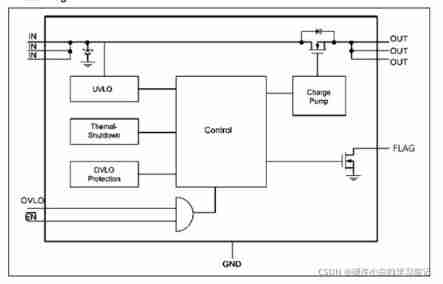
From the block diagram ,OVP The output voltage of , In essence, it is internal NMOS Tubular Uds. The maximum output voltage is NMOS Tubular DS Withstand voltage value .OVP The output of is disconnected , Nature is NMOS Disconnection and conduction of pipe .NMOS The opening and disconnection of pipes are mainly controlled by Vgs decision . However Vgs With Vin Change by change . This also has Vin Input range of .
Important parameter
Surge: Surge protection . There are some OVP Internal integration TVS, Therefore, it has certain surge protection function . General OVP The chip can resist 100V perhaps 120V Surge voltage , The biggest resistance of this chip 80V Surge voltage .
Vin: Input voltage , namely Vin Acceptable range of input voltage .
Vout: Output voltage , namely OVP Range of output voltage .
Rdson: Internal to the chip NMOS On resistance of . The lower the resistance, the better . Especially in the case of high current charging , It can reduce the pressure drop loss .
VIN_UVLO: namely OVP Minimum working voltage . When the input voltage reaches VIN_UVLO when ,OVP Turn on and start working , Its output has voltage .
VIN_OVLO: namely OVP Maximum working voltage . When the input voltage exceeds VIN_OVLO when ,OVP Disconnect the output of the stage after stopping , Its output has no voltage . It is controllable .
Isw, Input current , majority OVP chip , Input current MAX The value is 5V Even larger .
TOFF OVP Disconnect response time , It is often 50ns about . namely OVP The time between the input voltage exceeding the threshold and the output voltage breaking is 50ns.
Circuit design
If the default UovLo simply OVLO Pin ground .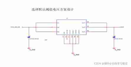
If you modify the threshold voltage by yourself , As shown in the figure . Through adjustment R1 And R2 Value , To adjust OVLO value .
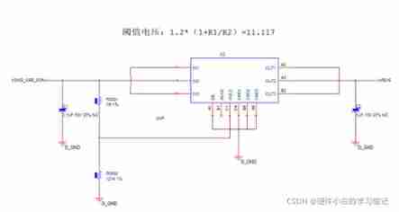
The input and output voltages in the figure above , The image can be displayed with an oscilloscope .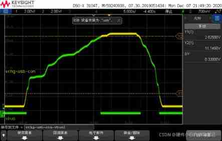
In terms of design , The capacitance at the input is also very particular . It is suggested to strictly follow datesheet It is required to select the tolerance . At the same time, the voltage withstand value , If there is TVS, Then the withstand voltage value should be greater than TVS The clamping voltage of . without TVS, It is better to choose the withstand voltage value as 50V, The capacity value is greater than or equal to 0.1uf The capacitance of . At the same time, the capacitance of the output , It is suggested to strictly follow datesheet choice , The withstand voltage value is greater than OVP The threshold voltage of . In previous projects , Most of us choose 0402 Encapsulated capacitor , Its withstand voltage value is also greater than that of the same type 0201 The capacitance of .
边栏推荐
- C WinForm [display real-time time in the status bar] - practical exercise 1
- Hardware 1 -- relationship between gain and magnification
- Mlperf training v2.0 list released, with the same GPU configuration, the performance of Baidu PaddlePaddle ranks first in the world
- 研究发现,跨境电商客服系统都有这五点功能!
- L'étude a révélé que le système de service à la clientèle du commerce électronique transfrontalier a ces cinq fonctions!
- The research found that the cross-border e-commerce customer service system has these five functions!
- Embedded composition and route
- UEFI development learning 4 - getting to know variable services
- Markdown tips
- UEFI development learning 3 - create UEFI program
猜你喜欢
Process communication mode between different hosts -- socket

UEFI development learning 5 - simple use of protocol
Volatile of C language

Basic embedded concepts

Matlab2018b problem solving when installing embedded coder support package for stmicroelectronic
![Shape template matching based on Halcon learning [vi] find_ mirror_ dies. Hdev routine](/img/99/21c228ff5de46c4a42b60f989b10e8.jpg)
Shape template matching based on Halcon learning [vi] find_ mirror_ dies. Hdev routine
Several implementation schemes of anti reverse connection protection of positive and negative poles of power supply!

Create inf module in AMI code
![Measurement fitting based on Halcon learning [i] fuse Hdev routine](/img/91/34c92065e797c87d6ce5ea13903993.jpg)
Measurement fitting based on Halcon learning [i] fuse Hdev routine

C#,数值计算(Numerical Recipes in C#),线性代数方程的求解,LU分解(LU Decomposition)源程序
随机推荐
Several implementation schemes of anti reverse connection protection of positive and negative poles of power supply!
【论文阅读】2022年最新迁移学习综述笔注(Transferability in Deep Learning: A Survey)
C WinForm [display real-time time in the status bar] - practical exercise 1
Factors affecting the quality of slip rings in production
1-stm32 operation environment construction
Solutions to compilation warnings in Quartus II
Talk about the circuit use of TVs tube
UEFI development learning 4 - getting to know variable services
Soem EtherCAT source code analysis II (list of known configuration information)
动力电池UL2580测试项目包括哪些
Sql Server的存储过程详解
Ads learning record (lna_atf54143)
Live555 push RTSP audio and video stream summary (III) flower screen problem caused by pushing H264 real-time stream
[trio basic tutorial 16 from introduction to proficiency] UDP communication test supplement
Hardware 1 -- relationship between gain and magnification
Ads usage skills
The research found that the cross-border e-commerce customer service system has these five functions!
PMSM dead time compensation
C WinForm [get file path -- traverse folder pictures] - practical exercise 6
C WinForm [change the position of the form after running] - Practical Exercise 4