当前位置:网站首页>[quick start of Digital IC Verification] 10. Verilog RTL design must know FIFO
[quick start of Digital IC Verification] 10. Verilog RTL design must know FIFO
2022-07-07 08:13:00 【luoganttcc】
Reading guide : The author has the honor to be a pioneer in the field of electronic information in China “ University of electronic technology ” During postgraduate study , Touch the cutting edge Numbers IC Verification knowledge , I heard something like Huawei Hisilicon 、 Tsinghua purple light 、 MediaTek technology And other top IC related enterprises in the industry , Pairs of numbers IC Verify some knowledge accumulation and learning experience . Want to get started for help IC Verified friends , After one or two thoughts , This column is specially opened , In order to spend the shortest time , Take the least detours , Most learned IC Verify technical knowledge .
List of articles
One 、 Sync FIFO
FIFO,First In First Out, First in, first out queue .
Learned to synchronize FIFO after , Then learn asynchronous FIFO It's easy to learn .
Study FIFO The requirements of , It is not required to be able to write completely , But understand the basic concepts ,FIFO What's the function , Design FIFO Basic requirements, etc
1.1、RAM(Random Access Memory) The design of the
Design and implement a 16x8 Dual port RAM
- RAM Width 8bit
- RAM depth 16
- ADDR A wide 2^4, Value range 0~15
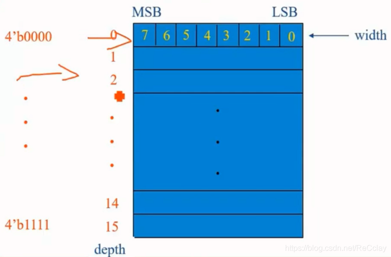
Corresponding code
module dp_ram(//dp = dual port
    input  wire                  write_clock,
    input  wire                  read_clock,
    input  wire                  write_allow,
    input  wire                  read_allow,
    input  wire [ADDR_WIDTH-1:0] write_addr,
    input  wire [ADDR_WIDTH-1:0] read_addr,
    input  wire [RAM_WIDTH-1:0 ] write_data,
    output reg  [RAM_WIDTH-1:0 ] read_data
);

    parameter DLY       = 1;
    parameter RAM_WIDTH = 8;
    parameter RAM_EDPTH = 16;
    parameter ADDR_WIDTH= 4;

    reg [RAM_WIDTH-1:0 ] memory[RAM_EDPTH-1:0];

    [email protected](posedge write_clock) begin
        if(write_allow)
            memory[write_addr] <= #DLY write_data;
    end

    [email protected](posedge read_clock) begin
        if(read_allow)
            read_data <= #DLY memory[read_addr];
    end

endmodule
1.2、 Sync FIFO The design of the
- FIFO principle : Can't write , Empty cannot read
- The key :full and empty How signals are generated
- Method 1: With length counter factor, Perform a write operation ,factor Add 1; Perform a read operation ,factor reduce 1.【 It will occupy more resources , But it is easy to realize 】
- Method 2: The address bit is extended by one bit , Use the highest position to judge whether it is full .【 Less resources , The implementation is a little more complicated 】
1.2.1、 Method 1 Corresponding
module SYNCFIFO(
    input   wire                        Fifo_rst,
    input   wire                        Clock,
    input   wire                        Read_enable,
    input   wire                        Write_enable,
    input   wire    [DATA_WIDTH-1:0]    Write_data,

    output   reg    [DATA_WIDTH-1:0]    Read_data,
    output   reg                        Full,
    output   reg                        Empty,
    output   reg    [ADDR_WIDTH-1:0]    Fcounter

);

    parameter DATA_WIDTH = 8;
    parameter ADDR_WIDTH = 9;

    reg [ADDR_WIDTH-1:0] Read_addr;
    reg [ADDR_WIDTH-1:0] Write_addr;

    wire Read_allow = (Read_enable && !Empty); // Empty cannot read ; It's better not to write like this , It's easy to make mistakes , This writing is equivalent to assign That kind of !
    wire Write_allow = (Write_enable && !Full); // Can't write

    DUALRAM U_RAM(
        .Write_clock    (Clock),
        .Read_clock     (Clock ),
        .Write_allow    (Write_allow),
        .Read_allow     (Read_allow ),
        .Write_addr     (Write_addr ),
        .Read_addr      (Read_addr  ),
        .Write_data     (Write_data ),
        .Read_data      (Read_data  )
    );

    [email protected](posedge Clock or posedge Fifo_rst)
        if(Fifo_rst)
            Empty <= 'b1;
        else
             It's a little complicated , as long as Fcounter[8:0]==9'h0, that Empty for 1 that will do !
            Empty <= (!Write_enable && (Fcounter[8:1]==8'h0) && ((Fcounter[0] == 0) || Read_enable) );

    [email protected](posedge Clock or posedge Fifo_rst)
        if(Fifo_rst)
            Full <= 'b1;
        else
            // It's also complicated , as long as Fcounter[8:0]==9'b1_1111_1111, that Full for 1 that will do !
            Full <= (!Read_enable && (Fcounter[8:1]==8'hFF) && ((Fcounter[0]==1) || Write_enable));

    [email protected](posedge clock or posedge Fifo_rst)
        if(Fifo_rst)
            Read_addr <= 'h0;
        else if(Read_allow)
            Read_addr <= Read_addr + 'b1;// It's better to add a boundary limit ,eg:if(Read_addr >= Depth-1) Read_addr <= 'h0 And so on. !

    [email protected](posedge clock or posedge Fifo_rst)
        if(Fifo_rst)
            Write_addr <= 'h0;
        else if(Write_allow)
            Write_addr <= Write_addr + 'b1;// It is also best to add a boundary limit

    [email protected](posedge clock or posedge Fifo_rst)
        if(Fifo_rst)
            Fcounter <= 'h0;
        else if((!Read_allow && Write_allow) || (Read_allow && !Write_allow))
        begin
            if(Write_allow) Fcounter <= Fcounter + 'b1;
            else    Fcounter <= Fcounter - 'b1;
        end

endmodule
- Follow RAM comparison ,FIFO Can't see the address , Only reading and writing are enabled , To produce in sequence RAM Address .
Little knowledge :RTL Code is not a program , Programs are compiled into instructions and data , Put it in memory , adopt CPU Take command 、 decoding 、 perform !RTL The code is not compiled , Comprehensive mapping into net table , Reflect the actual hardware circuit !
1.2.2、 Method 2 Corresponding Verilog Code
- Depth is 4 Of FIFO, Actual bit width 2bit That's enough , Expanding one becomes 3bit.
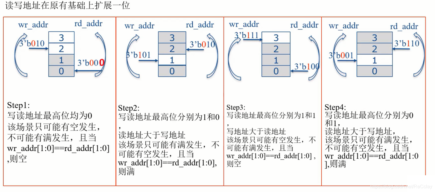
- scene 1 and 3, The highest bits of read and write are equal , namely w[2] = r[2], And w[1:0] = r[1:0],empty It works , It's empty .
- scene 2 and 4, The highest bit of reading and writing varies , namely w[2] != r[2], And w[1:0] = r[1:0],full It works , To be full .
- Expand to judge the scene !
module sync_fifo(
    input   wire            clk,
    input   wire            rst,
    input   wire            wr_en,
    input   wire            rd_en,
    input   wire    [7:0]   data_in,

    output  wire            empty,
    output  wire            full,
    output  reg     [7:0]   data_out,

);

reg  [7:0]  mem[15:0];
wire [3:0]  w_addr,r_addr;
reg  [4:0]  r_addr_a, w_addr_a; //16 Address depth ,4 Bit is enough, that is [3:0], here [4:0] Expanded 1 position


assign r_addr = r_addr_a[3:0];
assign w_addr = w_addr_a[3:0];

[email protected](posedge clk or negedge rst)
    if(!rst)
        r_addr_a <= 5'b0;
    else begin
        if(rd_en==1 && empty==0) begin
            data_out <= mem[r_addr];
            r_addr_a <= r_addr_a + 1;
        end
    end

[email protected](posedge clk or negedge rst)
    if(!rst)
        w_addr_a <= 5'b0;
    else begin
        if(wr_en==1 && full==0) begin
            mem[w_addr] <= data_in;
            w_addr_a <= w_addr_a + 1;
        end
    end

assign empty = (r_addr_a == w_addr_a) ? 1 : 0;
assign full  = (r_addr_a[4] != w_addr_a[4]  && r_addr_a[3:0] == w_addr_a[3:0]) ? 1 : 0;

endmodule
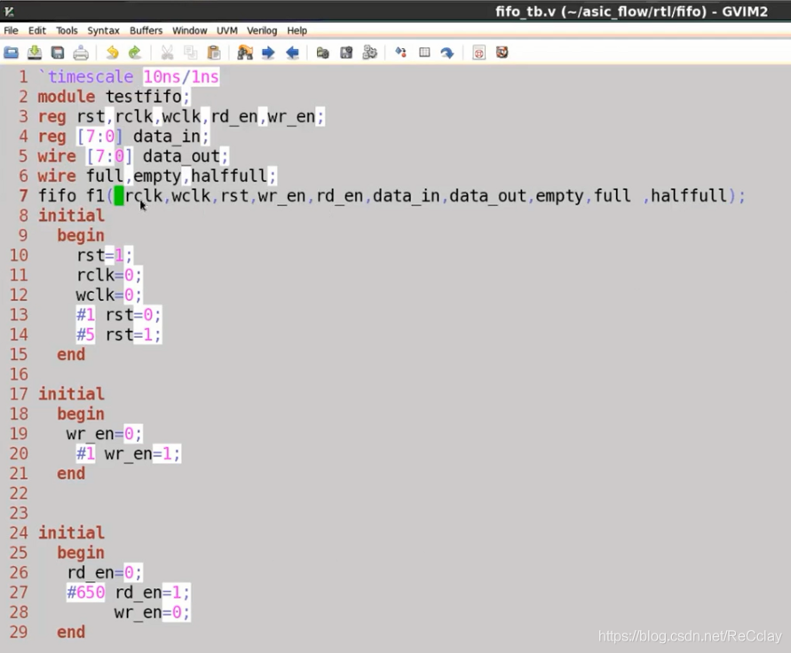
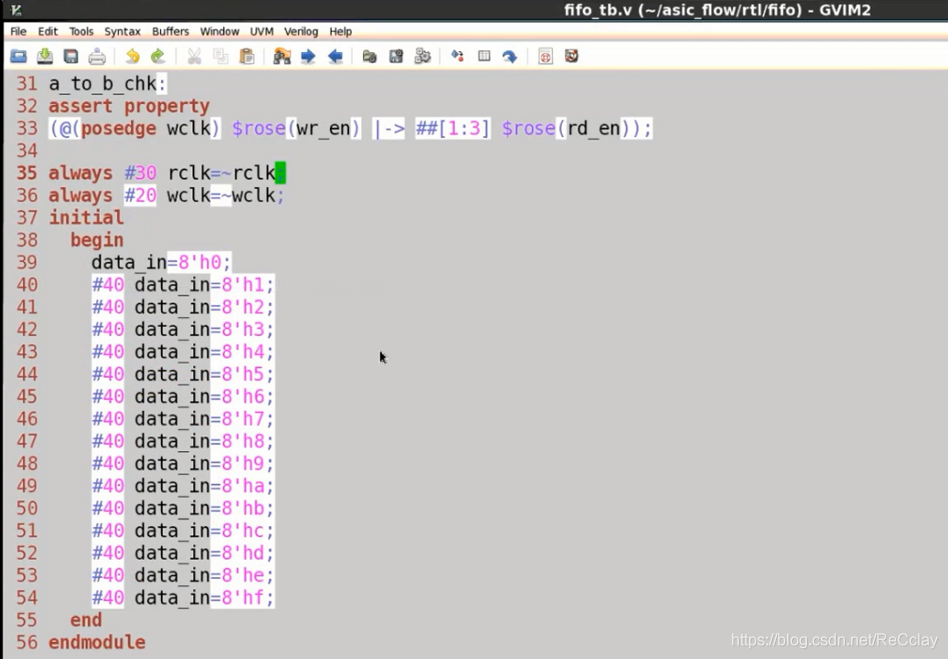
Corresponding TestBench
Two 、 asynchronous FIFO
- Use the way of expanding address bits to judge whether it is empty or full
- The clock of read-write signal is different
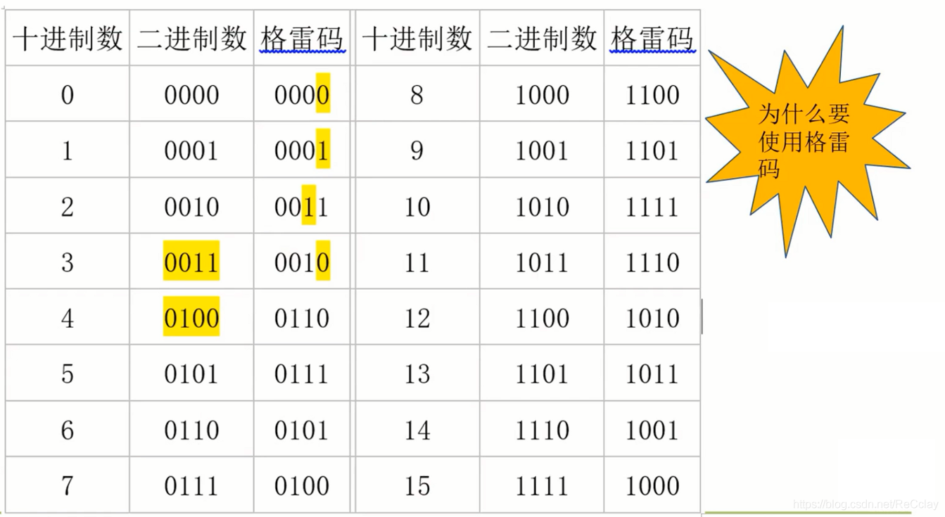
- The key : The use of gray code 【 asynchronous FIFO: Read and write clock fields are different 】【 Gray code : only one bit Jumping 】
- Read and write address conversion , Synchronize after conversion , In this way, the intermediate metastable state introduced by multi bit simultaneous flipping can be avoided !
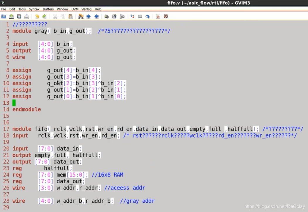
Gray code conversion module corresponds to RTL Code
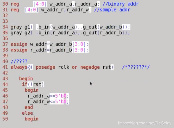
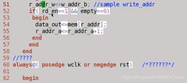
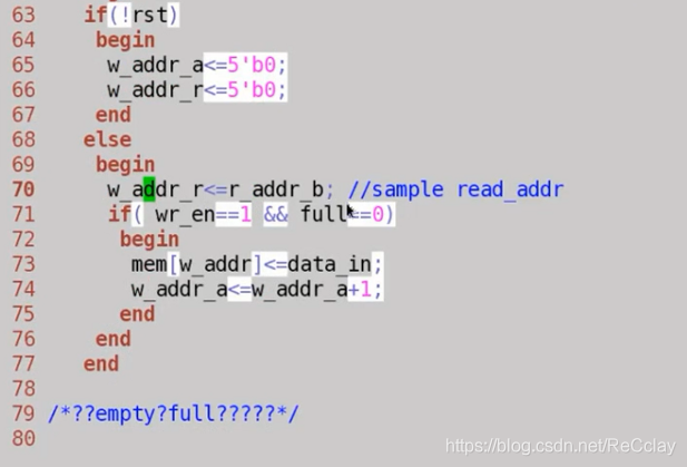

- Synchronize with FIFO Something different , To sample addresses across clock domains , Sampling goes through a gray code conversion , Otherwise, sampling will cause problems .
- Only one asynchronous clock is used here cycle De mining , In fact, in order to prevent metastable , Take three shots , This place is not standardized !
- EDA Generally, the simulation cannot check the asynchronous problem .
边栏推荐
- Network learning (II) -- Introduction to socket
- offer收割机:两个长字符串数字相加求和(经典面试算法题)
- QT learning 26 integrated example of layout management
- Openjudge noi 2.1 1752: chicken and rabbit in the same cage
- 发挥创客教育空间的广泛实用性
- Roulette chart 2 - writing of roulette chart code
- CDC (change data capture technology), a powerful tool for real-time database synchronization
- Offer harvester: add and sum two long string numbers (classic interview algorithm question)
- 2022 Inner Mongolia latest advanced fire facility operator simulation examination question bank and answers
- eBPF Cilium实战(2) - 底层网络可观测性
猜你喜欢

【数字IC验证快速入门】10、Verilog RTL设计必会的FIFO

漏洞复现-easy_tornado

Leetcode simple question: find the K beauty value of a number

央视太暖心了,手把手教你写HR最喜欢的简历

柯基数据通过Rainbond完成云原生改造,实现离线持续交付客户

在Rainbond中一键部署高可用 EMQX 集群
调用 pytorch API完成线性回归
![[quick start of Digital IC Verification] 15. Basic syntax of SystemVerilog learning 2 (operators, type conversion, loops, task/function... Including practical exercises)](/img/e1/9a047ef13299b94b5314ee6865ba26.png)
[quick start of Digital IC Verification] 15. Basic syntax of SystemVerilog learning 2 (operators, type conversion, loops, task/function... Including practical exercises)
【数字IC验证快速入门】14、SystemVerilog学习之基本语法1(数组、队列、结构体、枚举、字符串...内含实践练习)
在Rainbond中实现数据库结构自动化升级
随机推荐
offer收割机:两个长字符串数字相加求和(经典面试算法题)
The zblog plug-in supports the plug-in pushed by Baidu Sogou 360
Make LIVELINK's initial pose consistent with that of the mobile capture actor
拓维信息使用 Rainbond 的云原生落地实践
Qinglong panel -- Huahua reading
OpenVSCode云端IDE加入Rainbond一体化开发体系
Es FAQ summary
Explore dry goods! Apifox construction ideas
Unityhub cracking & unity cracking
Implementation of replacement function of shell script
Roulette chart 2 - writing of roulette chart code
解读创客思维与数学课程的实际运用
Avatary的LiveDriver试用体验
藏书馆App基于Rainbond实现云原生DevOps的实践
云原生存储解决方案Rook-Ceph与Rainbond结合的实践
Openjudge noi 2.1 1752: chicken and rabbit in the same cage
青龙面板--整理能用脚本
Zcmu--1492: problem d (C language)
Fast parsing intranet penetration escorts the document encryption industry
What is the function of paralleling a capacitor on the feedback resistance of the operational amplifier circuit