当前位置:网站首页>Altium Designer Basics
Altium Designer Basics
2022-08-02 05:02:00 【Fenghua classmate】
I'm currently learning about robotic arms,I found that the code of the six-axis robotic arm I bought is not very easy to use,And it doesn't quite fit your actual situation.因此学习PCB的相关知识,Going to draw a piece based on it myselfSTM32F103C8T6主控芯片的PCBdesign board,Schematic and schematics will be released laterPCBdesign board,欢迎大家一起交流学习!
AD的基础知识
1.学习方法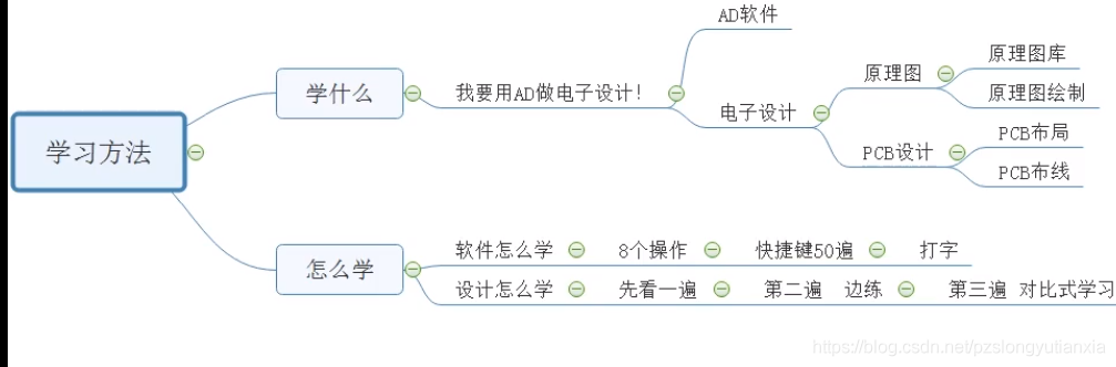
2.工程文件
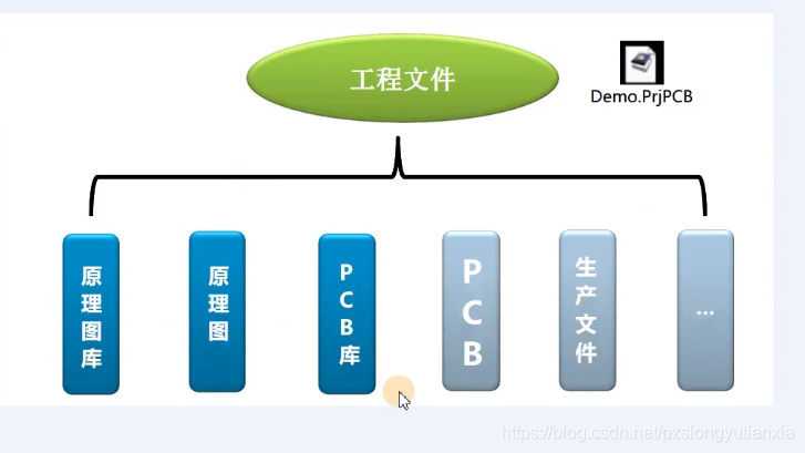
PCBA library is equivalent to onePCBTemplates are nested.
3.元件符号
The border of the element、管脚名称、元件名称、Component composition description(The serial numbers and names of the pins must be in one-to-one correspondence)
An explanation of the resistance and capacitance models
- Note that the component library must be created first(SCH Library),RES为电阻,而CAP为电容
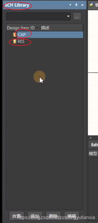
电阻

可以使用Tabkey to edit properties(名称,管脚号,pin shape, etc),Enter来确定
默认放100mil,按住shiftkey to copy and drag it
元件说明(Description):Can be hidden
电容
IC模型的绘制(芯片)
添加IC的型号:Use a rectangle to draw**
放置管脚–>使用tabkey to set it
移动(框选所有)–>按MS键
Designer:U?
Double-click the pin number to jump to the corresponding pinProperties中进行更改
Designer Item ID:Represents the model of the component
CommentFill in the model of the chip directly.如LM2633的型号为2633
按Pkey to place a pin
Pin name location
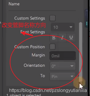
注意:
If there is when naming/则需要在name中添加\
Shortcut source:
- The combination of underscores is usede.g.TC
- A+L为左对齐
- A+Rfor right alignment and so on
- 自定义的话,Right click and set it,根据自己的需要进行设置
- The combination of underscores is usede.g.TC
Pin header class creation(座子)
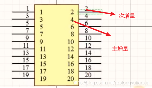
Displays the pin number(The name can be hidden,But the pin number is not recommended to be hidden),pin number andPCB的一一对应.
There are more pins in the pin header,使用阵列式粘贴to paste the pins in batches
- Choose a pin:CTRL+C复制,Then set Paste Array in the Edit menu bar
排针Designer:J?
Creation of optocouplers and diodes
二极管
- 二极管:先使用多边形工具Draw the border,Then set the border(颜色和大小).Then use the Polygon Tool to draw rectangles(Double-click the property to set the internal color).
- Used when paintingsmallest来进行绘制
- The view can be set to when drawing the diode's rectangle1mil来进行操作,Then adjust it back.
- Designer:D?
光耦

- Arrows are drawn using lines
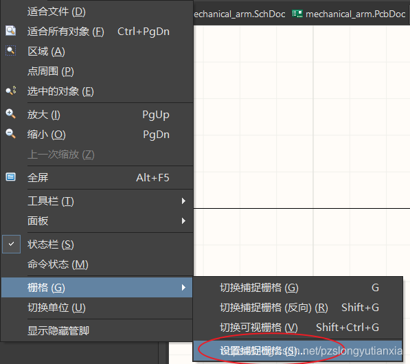
- Relevant adjustments can be made by setting the grid points
- Designer:U?
注意:可以调整为20mil进行绘制,镜像:在复制的情况下,按ymakes mirroring.Alignment is possible when the grid points are the same
4.Make a call with an existing model
在设计–>Generated in the schematic library,Use Generate Schematic Library,Generate component models.
- The meaning of this figure is the default classification of a component model

- Using one or more components from a schematic library,just do it directly复制粘贴就行.
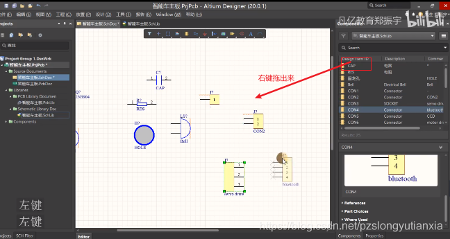
5.component placement
- Open the component library to place the components in it.There is a place in the lower left corner to place components into the schematic.也可以打开ComponentDo a drag and drop on the component
6.Device duplication and alignment
Schematic resizing:Click the border to choose a size to resize.e.g.调整为A3纸
移动元器件:M+S移动元器件;Press and hold the space to perform a rotating placement
When drawing, the components are generally placed in a specific position.
- 使用shift+Space to toggle the shape of the line,For example, a right angle is converted to a straight angle.
If there is no component in the schematic library,You can create a component yourself.Then make one more addition.
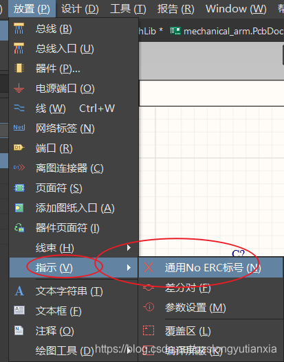
7.wire andNetlabel的添加
导线:CTRL+W(Has electrical propertiesThe line is not the same as the ordinary auxiliary line)
Press the backspace key to remove the excess wire.
网络标签:Netlabel的添加—>It is equivalent to binding names to certain components or pins
In general, components are updated in the schematic library,Then update the schematic library.
8.Value值的核对
- 编辑位号:从左往右,从上往下进行编号.The tag number can be changed automatically,Set the starting bit number by yourself.–>Indicates the location of the component.Finally, make a modification by yourself and correspond to the bit number on the schematic diagram one by one

极性,标号,Value值,连接属性,Network labels are checked
- valueThe value represents the size of the value of the component,Check according to the actual situation、调整
9.封装的统一管理:原理图与PCBMapping of the board
通过封装管理器Make a change.
- 在添加栏Change the package uniformly

- 根据boomFill out the form for the package
10.Schematic inspection、编译
检查错误
Common types of errors and engineering errors
Missing values can be viewed in the footprint manager(Sort by serial number)
网络悬浮:The location of the network is incorrect
单端网络(one point net work):When two identical network labels are connected together.单端网络不一定有问题,根据实际情况决定.
- Eliminate single-ended networks
- Eliminate single-ended networks
11.常见的CHIP的封装(电阻、电容、SOT、二极管)
- PCB封装:Mapping body between electronic design drawings and physical objects,With precise data requirements
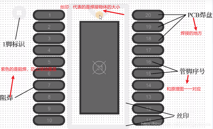
注:1The pin marks indicate the forward and reverse directions of the device.The solder mask copper is exposed,Welding for welding,The pads must have solder mask.
- Pad selection
- It is selected via the parameter table,The relevant distance is selected by the specification parameter
- 丝印
- Draw on both sides of the pad,Use polarity judgment
12.常见的IC类封装
阵列粘贴
通过X/YThe offset is used to move the component.
E+KMake a silkscreen cut
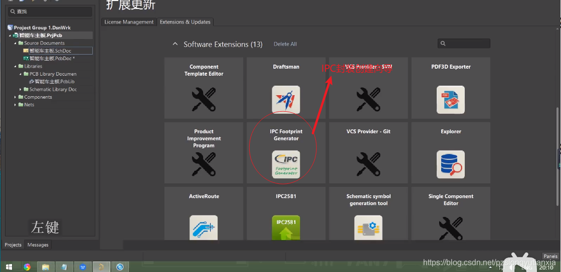
13.利用IPCWizard to quickly create footprints:创建好2D和3D图像
- Download in the extension

14.常用的PCB封装直接调用
生成PCB库:将我们的PCB板子,直接使用DPto make a buildPCB模型.可以直接使用PCB的库.
在PCB中进行Ctrl+cThen do it in the list of componentsCtrl+v(Don't do it on our pageCtrl+v)
学习心得:关于ADThe basics in the book can be quickly read,Then do practical exercises,Find mistakes in practice、Acquire new knowledge!
以上是ADBasic usage of the software,The next article will be about actual combatADbasic knowledge required.顺便在这里cueOne by one aboutAD的基础视频,讲的非常详细Altium Designer 20 19(入门到精通全38集)四层板智能车PCB设计视频教程AD19 AD20 凡亿教育
边栏推荐
- 联阳IT66121FN提供SDI转HDMI方案分享
- 【TCS3200 color sensor and Arduino realize color recognition】
- 基础IO(上):文件管理和描述符
- R语言 —— 多元线性回归
- 字符串匹配(蛮力法+KMP)
- 2020 - AAAI - 图像修复 Image Inpainting论文导读 -《Region Normalization for Image Inpainting》
- Introduction and mock implementation of list:list
- ICN6211:MIPI DSI转RGB视频转换芯片方案介绍 看完涨知识了呢
- 【科普贴】SPI接口详解
- openwrt RK3568_EVB移植
猜你喜欢


随机推荐
Arduino lights up nixie tubes
ICN6211:MIPI DSI转RGB视频转换芯片方案介绍 看完涨知识了呢
Anaconda(Jupyter)里发现不能识别自己的GPU该怎么办?
【面试必看】链表的常见笔试题
GM8775C MIPI转LVDS调试心得分享
Comparative analysis of mobile cloud IoT pre-research and Alibaba Cloud development
TeamCode 产品 UI 全新升级,快来体验吧
GM8775C MIPI转LVDS调试资料分享
分割回文串 DP+回溯 (LeetCode-131)
D类音频功放NS4110B电路设计
IoT solution
GM8284DD,GM8285C,GM8913,GM8914,GM8905C,GM8906C,国腾振芯LVDS类芯片
使用buildroot制作根文件系统(龙芯1B使用)
2020 - AAAI - 图像修复 Image Inpainting论文导读 -《Region Normalization for Image Inpainting》
[Arduino uses a rotary encoder module]
字符串匹配(蛮力法+KMP)
proteus数字电路仿真——入门实例
NE5532运放加法器
uniCloud use
回溯法 & 分支限界 - 2