当前位置:网站首页>Digital IC Design SPI
Digital IC Design SPI
2022-07-07 13:17:00 【Tung flower】
SPI Bus concept
SPI ( Serial Peripheral Interface, Serial peripheral interface ) It's a kind of synchronization 、 full duplex 、 Master slave mode , High speed interface (UART Is asynchronous ).
From the host or Slave The data of is synchronized on the rising or falling edge of the clock . The master and slave can transmit data at the same time .
Serial peripheral interface (SPI) application :
Serial peripheral interface (SPI) Microcontrollers and peripherals IC( Such as sensor 、ADC、DAC、 shift register 、SRAM etc. ) One of the most widely used interfaces between .
SPI The bus has the following characteristics :
- Less connection , Simplify circuit design . Parallel bus expansion methods usually require 8 Data line 、8~16 Root address line 、2~3 A control line . And this design , Only 4 Root data and control line can complete the functions realized by parallel expansion .
- Devices are uniformly addressed , And has nothing to do with the system address , operation SPI Good independence .
- The operation of devices shall comply with unified specifications , Make the system software and hardware have good versatility .
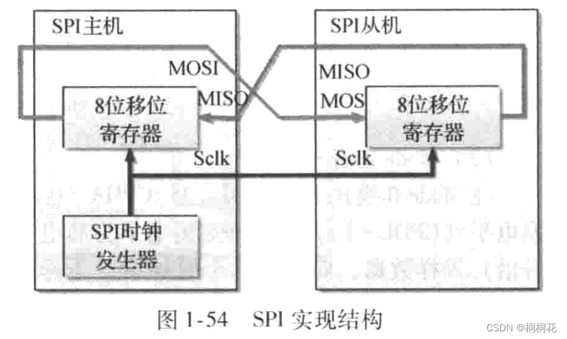
SPI System architecture of bus
SPI It's a ring bus structure , from SS(CS)、SCK、MOSI、MISO constitute , Mainly in the SCK Under the control of , Two bidirectional shift registers exchange data .
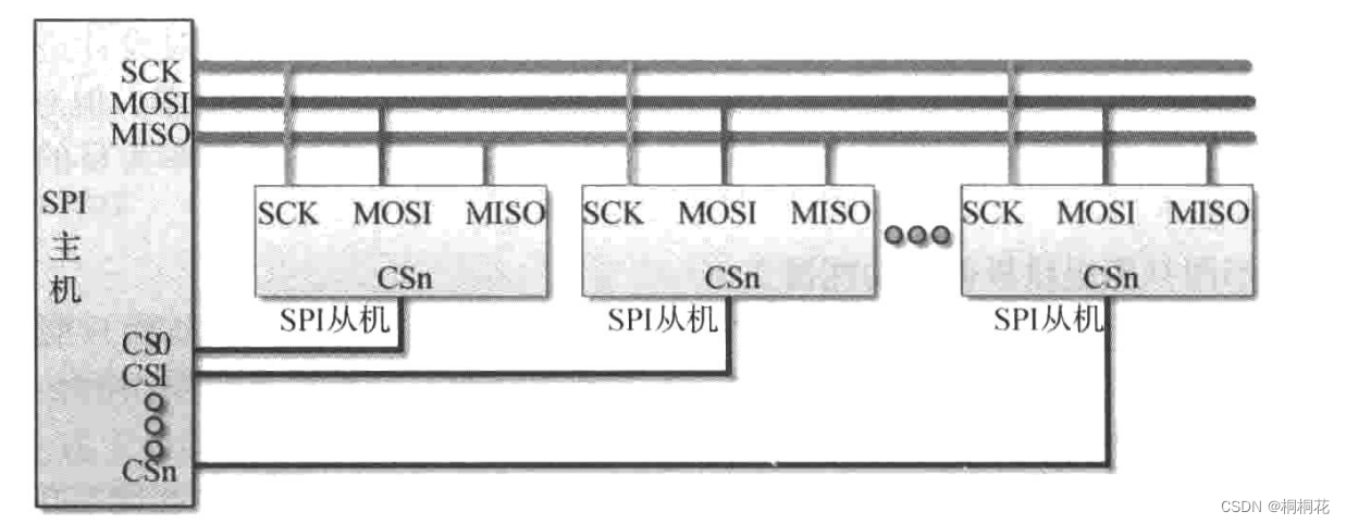
SPI The signal :

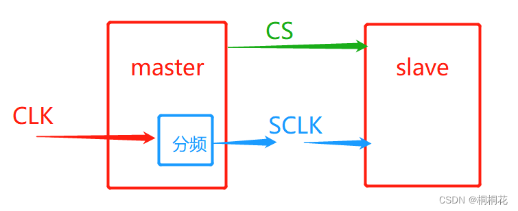
- The clock ((Serial Clock,SCK)SPI CLK,SCLK): The device that generates the clock signal is called the host .
- Piece of optional signal ( Peripheral device chip selection signal line (Slave Selection,SS)CS): Slave enable signal , Controlled by the host .. The chip selection signal from the host is used to select the slave .( This is usually a low level active signal , When pulling up, the slave and SPI The bus is disconnected . When using multiple slaves , The master needs to provide a separate chip selection signal for each slave .)
- Host output 、 Slave input ((Master Out Slave In,MOSI)MOSI): cable , Send data from the host to the slave .
- Host input 、 Slave output ((Master In Slave Out,MISO)MISO): cable , Send data from slave to host .
The relationship between master and slave :
- The data transmitted between the master and the slave is synchronized with the clock generated by the master .
- SPI The interface can only have one host , But there can be one or more slaves .
SPI The data transfer
SPI The data transmission is in the serial synchronization clock signal (Serial Clock,SCK) Under the control of .
SPI How to ensure synchronization :
On the one hand, the clock generator of the host controls the shift register of the host , On the other hand, through the slave SCK Signal line to control the shift register of the slave , So as to ensure that the data exchange between the master and the slave is synchronized .
SPI Start communicating
Host send Clock signal .
The host is enabled Piece of optional signal CS( Low level active ) Select slave .
SPI During the communication
SPI Both the master and slave of the bus have a shift register .
When the host writes data to its shift register , The data will go through MOSI The signal line Enter the shift register of the slave ;
meanwhile ,
Data in the slave shift register , adopt MISO The signal line Enter the shift register of the host .
such , The master and slave complete a data exchange .
Be careful :
SPI It's a full duplex interface , The master and slave can pass through MOSI and MISO The line sends data at the same time .【 Data transmission ( Serial move out to MOSI/SDO On the bus ) And receiving ( Sample or read into the bus (MISO/SDI) The data on the ) At the same time .】
Serial clock edge Sync Data shift and sampling .
SPI The interface allows users to flexibly select the rising edge or falling edge of the clock to sample and output / Or shift data .
Four kinds of SPI Pattern
Clock phase (CPHA) And clock polarity (CPOL)
SPI The serial synchronization clock can be set to different polarity (Clock Polarity ,CPOL) And phase (Clock Phase ,CPHA).
The polarity of the clock (CPOL)
Used to determine when the bus is idle , Synchronous clock (SCK) Whether the potential on the signal line is high or low .
- At that time, the polarity of the clock was 0 when (CPOL=0),SCK The signal line is Idle by Low level
- At that time, the polarity of the clock was 1 when (CPOL=1),SCK The signal line is Idle by High level
Idle state :
At the beginning of the transmission CS It is high level and during the transition to low level ,
At the end of the transmission CS It is low level and during the transition to high level .
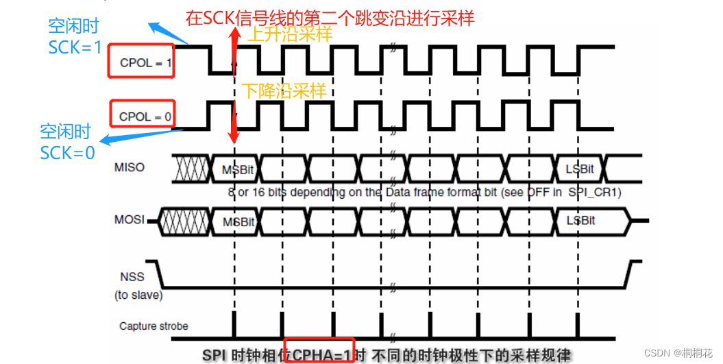
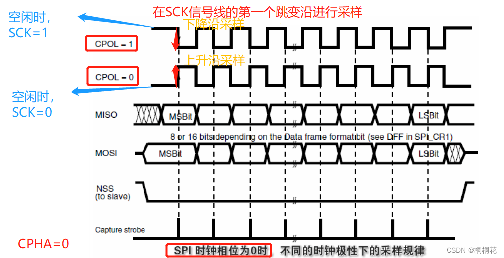
The phase of the clock (CPHA)
Clock edge for reading data and sending data ( Rising edge or falling edge ).
CPHA=1( stay SCK The second jump edge of the signal line is sampled )
- At that time, the polarity of the clock was 0 when (CPOL=0), take Falling edge
- At that time, the polarity of the clock was 1 when (CPOL=1), take Rising edge
CPHA=0( stay SCK Sample the first jump edge of the signal line )
- At that time, the polarity of the clock was 0 when (CPOL=0), take Rising edge
- At that time, the polarity of the clock was 1 when (CPOL=1), take Falling edge
Four kinds of SPI Pattern
The master must select the clock polarity and clock phase according to the requirements of the slave .
according to CPOL and CPHA The choice of bits , There are four kinds. SPI Mode available .
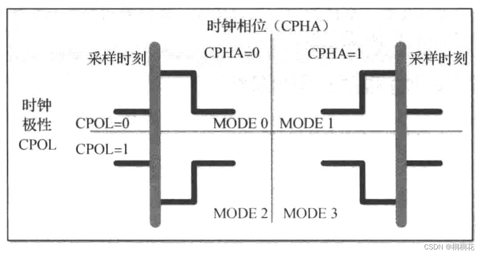
| SPI Pattern | CPOL | CPHA | Clock polarity in idle state | For sampling and / Or move the clock phase of the data |
| 0 | 0 | 0 | Logic low level | Rising edge sampling , The falling edge moves out |
| 1 | 0 | 1 | Logic low level | Falling edge sampling , The rising edge moves out |
| 2 | 1 | 0 | Logic high level | Falling edge sampling , The rising edge moves out |
| 3 | 1 | 1 | Logic high level | Falling edge sampling , The rising edge moves out |
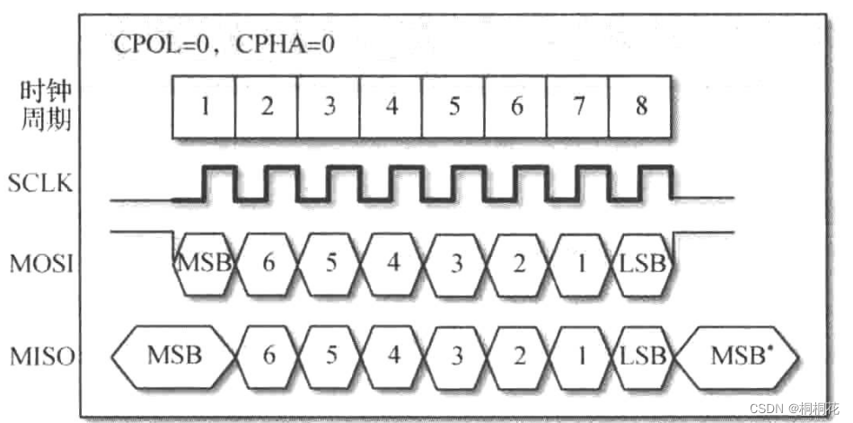
Mode0:CPOL= 0,CPHA = 0:( stay SCK Sample the first jump edge of the signal line )
CPOL =0 :
The clock remains low before and after data transmission ( The idle level of the clock is low )
CPHA =0:
On the first clock edge ( Rising edge ) Sampled data ,
On the second clock edge ( Falling edge ) Output data .
MODE0 The transmission timing of :
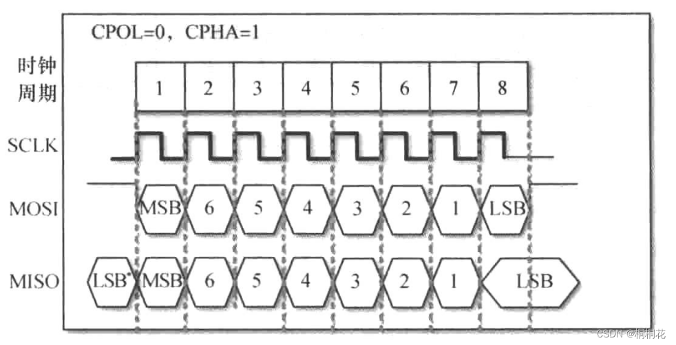
Mode1:CPOL = 0,CPHA = 1:( stay SCK The second jump edge of the signal line is sampled )
CPOL =0 :
The clock remains low before and after data transmission ( The idle level of the clock is low )
CPHA =1:
On the second clock edge ( Rising edge ) Sampled data ,
On the first clock edge ( Falling edge ) Output data .
MODE1 The transmission timing of :
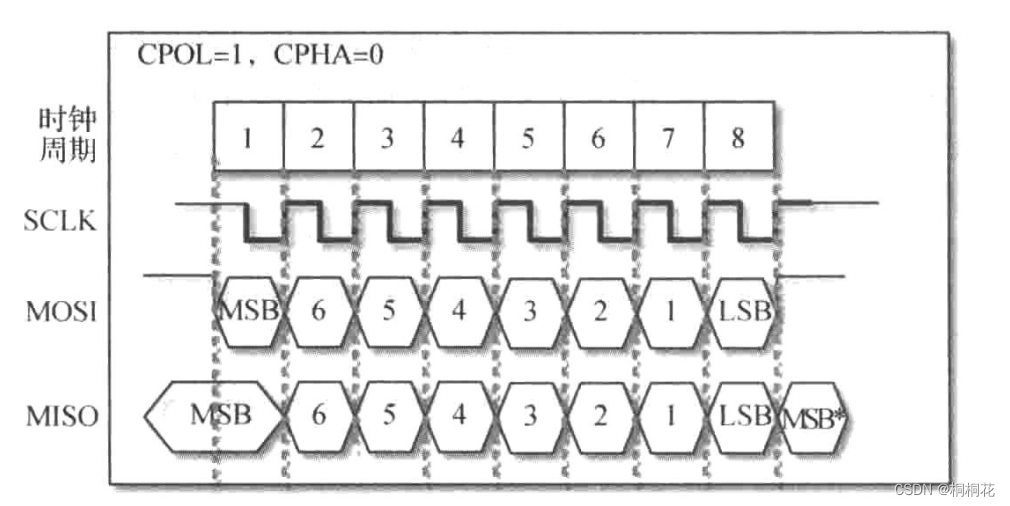
Mode2:CPOL= 1,CPHA = 0:( stay SCK Sample the first jump edge of the signal line )
CPOL =1:
The clock remains high before and after data transmission ( The idle level of the clock is high )
CPHA =0:
On the first clock edge ( Rising edge ) Sampled data ,
On the second clock edge ( Falling edge ) Output data .
MODE2 The transmission timing of :
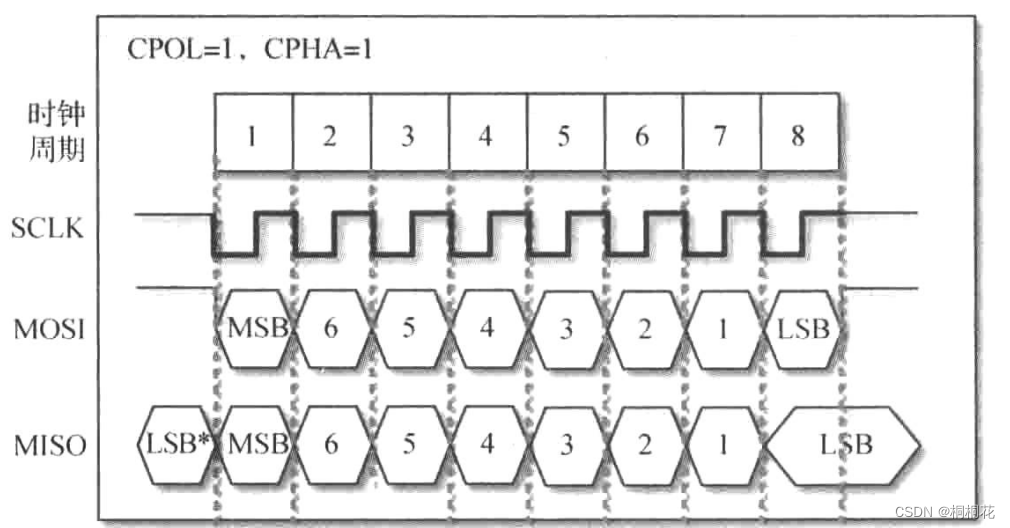
Mode3:CPOL = 1,CPHA = 1:( stay SCK The second jump edge of the signal line is sampled )
CPOL =1:
The clock remains high before and after data transmission ( The idle level of the clock is high )
CPHA =1:
On the second clock edge ( Rising edge ) Sampled data ,
On the first clock edge ( Falling edge ) Output data .
MODE3 The transmission timing of :
SPI sequential

Set the rising edge to send 、 Falling edge reception 、 High bits send first .
※ Clock polarity and clock phase are two choices :
- CPHA = 0,CPOL = 1
- CPHA = 1,CPOL = 0
※ According to the chip selection signal CS Select slave
※SPI sequential
Master and slave initialization is ready
Host register =0xaa=10101010
Slave register =0x55 =01010101
When the first rising edge comes
MOSI=1; Host register =0101010x
MISO=0; Slave register =1010101x
When the first falling edge comes
MOSI Passed to the slave register , Slave register =0101010MOSI=01010101
MISO Passed to the host register , Host register =0101010MISO=01010100
8 After a clock pulse , The contents of the two registers are exchanged with each other once .
Host register =01010101
Slave register =10101010
This completes one of the SPI sequential .
Based on the above analysis , A complete transmission cycle is 16 position , Two bytes .
explain :
The host sends a command first , Then the slave prepares data according to the host name ,
The host is next 8 Bit clock cycle to read data back
| pulse | Host register master buffer | Slave slave buffer | MISO | MOSI |
| 0 | 10101010 | 01010101 | 0 | 0 |
| The first 1 Pulse rising edge ( send out ) | 0101010x | 1010101x | 0 | 1 |
| The first 1 Pulse falling edge ( receive ) | 01010100 | 10101011 | 0 | 1 |
| The first 2 Pulse rising edge ( send out ) | 1010100x | 0101011x | 1 | 0 |
| The first 2 Pulse falling edge ( receive ) | 10101001 | 01010110 | 1 | 0 |
| The first 3 Pulse rising edge ( send out ) | 0101001x | 1010110x | 0 | 1 |
| The first 3 Pulse falling edge ( receive ) | 01010010 | 10101101 | 0 | 1 |
| The first 4 Pulse rising edge ( send out ) | 1010010x | 0101101x | 1 | 0 |
| The first 4 Pulse falling edge ( receive ) | 10100101 | 01011010 | 1 | 0 |
| The first 5 Pulse rising edge ( send out ) | 0100101x | 1011010x | 0 | 1 |
| The first 5 Pulse falling edge ( receive ) | 01001010 | 10110101 | 0 | 1 |
| The first 6 Pulse rising edge ( send out ) | 1001010x | 0110101x | 1 | 0 |
| The first 6 Pulse falling edge ( receive ) | 10010101 | 01101010 | 1 | 0 |
| The first 7 Pulse rising edge ( send out ) | 0010101x | 1101010x | 0 | 1 |
| The first 7 Pulse falling edge ( receive ) | 00101010 | 11010101 | 0 | 1 |
| The first 8 Pulse rising edge ( send out ) | 0101010x | 1010101x | 1 | 0 |
| The first 8 Pulse falling edge ( receive ) | 01010101 | 10101010 | 1 | 0 |
SPI Design of functional modules
SPI The Lord of 、 From the inside of the equipment, there is one 8 Bit shift register .
In actual implementation , You can use the host Sclk Signal as shift clock signal , Follow the high order , The order of the lower order , Send the data on the bus into the internal shift register in turn , To complete the SPI Receiving and sending of .
design spec
1. SCLK use 10MHz
2. Module working clock 100MHz
3. When the received serial data is subject to serial parallel conversion , Feed back the parallel data to the upper module
4、 use CPOL = 0 ,CPHA = 1
CPOL =0 :
The clock remains low before and after data transmission ( The idle level of the clock is low )
CPHA =1:
On the first clock edge ( Rising edge ) Sampled data ,
On the second clock edge ( Falling edge ) Output data .
SPI Of SCLK Signal generation
Module clock CLK, frequency F=100MHz , Clock cycle =10ns
SCLK, frequency f=10MHz , Clock cycle =100ns (10 frequency division )
// Module clock :clk
//spi The clock :sclk
// Reset signal :rst_n
// A counter that counts the number of clocks :clk_cnt
//CPOL =0 ( The clock remains low before and after data transmission ( The idle level of the clock is low ))

[email protected](posedge clk or negedge rst_n)
 begin
  if(!rst_n)
     clk_cnt<=0;
     sclk<=0;
  else
     begin
     //(10 frequency division /2-1)
       if(clk_cnt==4'd4)
          begin
            sclk<=~sclk;
            clk_cnt<=0;
          end
       else
         begin
          clk_cnt<=clk_cnt+1;
         end
     end
master Simultaneous sampling and output
//master send data
[email protected](negedge sclk or negedge rst_n)
 begin
  if(!rst_n)
    mosi<=1'b1;
  else if(spi_done)
    mosi<=1'b1;
  else(!sclk&&!cs)
    begin
     mosi<=master_buf[7];
    end
end
//master receive data
[email protected](posedge sclk or negedge rst_n)
 begin
  if(!rst_n)
     master_buf[7:0]<=8'b0;
  else if(spi_done)
     master_buf[7:0]<=8'b0;
  else(!sclk&&!cs)
    begin
     master_buf[7:0]<={master_buf[6:0],miso};
    end
 end
slave Simultaneous sampling and output
//slave send data
[email protected](negedge sclk or negedge rst_n)
 begin
  if(!rst_n)
    miso<=slave_buf[0];
  else if(spi_done)
    miso<=slave_buf[0];
  else(!sclk&&!cs)
    begin
     miso<=slave_buf[7];
    end
end
//slave receive data
[email protected](posedge sclk or negedge rst_n)
 begin
  if(!rst_n)
     slave_buf[7:0]<=8'b0;
  else if(spi_done)
     slave_buf[7:0]<=8'b0;
  else(!sclk&&!cs)
    begin
     slave_buf[7:0]<={slave_buf[6:0],mosi};
    end
 end
Reference resources :
SPI Interface profile - simulation / Power Supply - -EETOP- Chuangxin net
How to understand SPI Polarity of bus clock (COL) And phase (CPHA)? - You know (zhihu.com)
边栏推荐
- Analysis of DHCP dynamic host setting protocol
- Lingyunguang of Dachen and Xiaomi investment is listed: the market value is 15.3 billion, and the machine is implanted into the eyes and brain
- 我那“不好惹”的00后下属:不差钱,怼领导,抵制加班
- 滑轨步进电机调试(全国海洋航行器大赛)(STM32主控)
- 【等保】云计算安全扩展要求关注的安全目标和实现方式区分原则有哪些?
- clion mingw64中文乱码
- 单片机原理期末复习笔记
- Go语言学习笔记-结构体(Struct)
- Cmu15445 (fall 2019) project 2 - hash table details
- regular expression
猜你喜欢
Cinnamon 任务栏网速
![[learning notes] zkw segment tree](/img/18/21f455a06e8629243fc5cf4df0044c.png)
[learning notes] zkw segment tree
共创软硬件协同生态:Graphcore IPU与百度飞桨的“联合提交”亮相MLPerf
Isprs2021/ remote sensing image cloud detection: a geographic information driven method and a new large-scale remote sensing cloud / snow detection data set
Vscade editor esp32 header file wavy line does not jump completely solved
滑轨步进电机调试(全国海洋航行器大赛)(STM32主控)
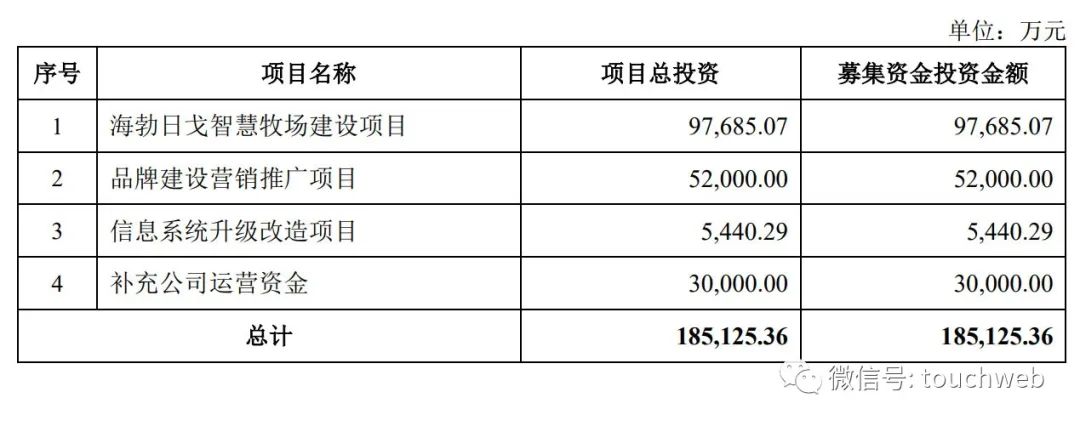
Adopt a cow to sprint A shares: it plans to raise 1.85 billion yuan, and Xu Xiaobo holds nearly 40%
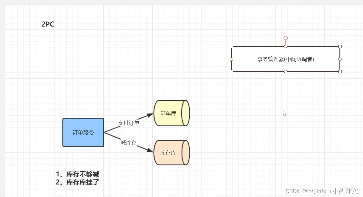
分布式事务解决方案
![[untitled]](/img/6c/df2ebb3e39d1e47b8dd74cfdddbb06.gif)
[untitled]
Milkdown 控件图标
随机推荐
迅为iTOP-IMX6ULL开发板Pinctrl和GPIO子系统实验-修改设备树文件
TPG x AIDU|AI领军人才招募计划进行中!
Awk of three swordsmen in text processing
Day26 IP query items
Per capita Swiss number series, Swiss number 4 generation JS reverse analysis
shell 批量文件名(不含扩展名)小写改大写
DETR介绍
Aosikang biological sprint scientific innovation board of Hillhouse Investment: annual revenue of 450million yuan, lost cooperation with kangxinuo
抓细抓实抓好安全生产各项工作 全力确保人民群众生命财产安全
. Net ultimate productivity of efcore sub table sub database fully automated migration codefirst
ESP32 ① 编译环境
基于鲲鹏原生安全,打造安全可信的计算平台
【无标题】
DHCP 动态主机设置协议 分析
About how appium closes apps (resolved)
About the problem of APP flash back after appium starts the app - (solved)
MySQL master-slave replication
MySQL入门尝鲜
[learning notes] segment tree selection
JS判断一个对象是否为空