当前位置:网站首页>Summary of SIM card circuit knowledge
Summary of SIM card circuit knowledge
2022-07-05 08:09:00 【Learning notes of hardware Xiaobai】
USIM yes Universal Subscriber Identity Module( Global subscriber identity card ) Abbreviation . Global user identity module (USIM), Also called upgrade SIM , Is in UMTS( Its full name is Universal Mobile Telecommunication System – General wireless communication system ) 3G A component of the network . Generally also refers to SIM card .
USIM Card structure
USIM The card is mainly composed of five parts . Respectively :CPU, Program memory ROM, Working memory RAM, Data storage EEPROM And serial communication unit .
SIM Card storage
In daily use of mobile phones , We will find that , Some mobile phone numbers or text messages , Call record , It will be displayed in different mobile phones with the mobile phone card . So that explains it SIM The card itself has a certain storage space . But different SIM Khaki capacity is different , It's usually 32K,64K as well as 128K.
SIM Card size
Buying SIM Card time , We all know , It is divided into three sizes .
The standard SIM card Size 15X25mm
Micro SIM Card size 15X12mm
Nan0 SIM card Size 12.3X8.8mm
SIM Card circuit
SIM The card circuit is mainly divided into the following parts
VCC: Power Supply , There is 1.8V/3V/5V, according to the agreement , What is commonly used at present is CLASS B And CLASS C . among :CLASS B Voltage is 2.7-3.3V.CLASS C Voltage is 1.62-1.98V. Power consumption CLASS B The maximum is 6mA.CLASS C The maximum is 4mA. In general ,SIM Card detection circuit requires support 1.8V And 3.0V.
RST: Reset , Used to reset the internal processor . Low level :0-0.2VCC. High level :0.8VCC-VCC.
CLK: The clock , The clocks are 1-4MHZ. Low level :0-0.2VCC. High level :0.7VCC-VCC.
IO, data Communication line for information transmission with the inside of the mobile phone . Low level :-0.3-0.2VCC. High level :0.7VCC-VCC+0.3.
VPP,SIM Programming power supply of card . In general NC, When the equipment has NFC This pin will be used in case of function .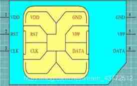
DET, Test pins , Low level unplug , High level insertion .
among ,DET Feet are not SIM Card pin signal . It only exists on the connector holder , It belongs to mechanical pin , The state switching between card inserting and card pulling is realized through the mechanical structure .
SIM Circuit design of card holder 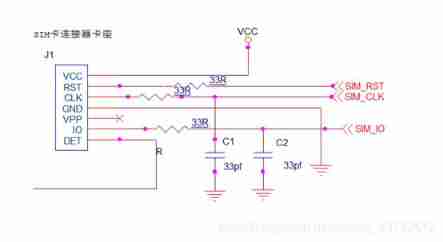
However, in terms of mobile tablets This connector base is not so . Everyone should know , Current mobile phone card slot , It not only supports the release of single cards , Double card , You can also put SD card , So the seats in this area are also very exquisite .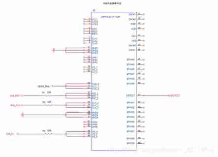
( The figure shows only the single card part ,SD The card part is not drawn )
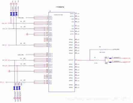
except VCC And GND outside , Other signals are directly connected to CPU.
On some circuits on the Internet , We may see Adding TVS tube , To prevent surge breakdown . However, in the field of mobile tablet that Xiaobian is engaged in ,TVS Not much is added , On the one hand, low capacity TVS It can deal with surge and electrostatic problems , But on the other hand, it increases the cost . Low volume TVS Tube prices are often higher than ordinary TVS Expensive . meanwhile , According to the experience of a large number of projects ,SIM Most of the cards are not added TVS Tube case , It can also be used in surge test and electrostatic test PASS. therefore When designing this aspect , If you are not sure whether to add , You can reserve TVS Tube position , Don't post it in the early stage , Then conduct surge electrostatic test , It depends on the result to decide whether to add !
If you really insist on adding . In fact, we should pay attention to some matters .
In circuit TVS capacitance resistance The selection
Capacitance CLK IO When processing line filtering , The capacity value cannot be too large . Too large not only has no ability to filter out RF interference , And it will cause the signal waveform to slow down , Serious cases will lead to card reading failure . Usually choose 33pf capacitance .
The termination resistance should not be too large , It leads to the decline of signal driving ability and abnormal waveform ,33R More resistors are used .
In some anti surge electrostatic measures , Will add some TVS tube .TVS Select the low volume value of the tube , Too much capacitance will cause the waveform to slow down , Card reading failed .
Layout Summary :
take esd The protective device is placed near the corresponding pin . if necessary rc Filter , Please place it in the corresponding esd Protective devices .
sim The routing of the card interface is 10CM Or shorter .
take sim The card signal is isolated from other high-speed signals , Parcel handling , To prevent high signal reception sim The speed signal affected by the card .
SIM The routing of cards is best to go together in a group .
The wiring should be on the inner layer as much as possible .
The capacitance should be close SIM Place the card pad .
SIM In the card CLK The line must be wrapped .
边栏推荐
- My-basic application 2: my-basic installation and operation
- Volatile of C language
- Define in and define out
- Network communication model -- Network OSI tcp/ip layering
- Detailed explanation of pragma usage
- Network port usage
- Wifi-802.11 negotiation rate table
- [tutorial 15 of trio basic from introduction to proficiency] trio free serial communication
- Semiconductor devices (III) FET
- [trio basic tutorial 17 from getting started to mastering] set up and connect the trio motion controller and input the activation code
猜你喜欢
![C WinForm [exit application] - practice 3](/img/25/30c795cc3fa6931eb1d733719d4ad0.jpg)
C WinForm [exit application] - practice 3
Why is 1900 not a leap year
Some thoughts on extracting perspectives from ealfa and Ebeta
【论文阅读】2022年最新迁移学习综述笔注(Transferability in Deep Learning: A Survey)
Wifi-802.11 negotiation rate table

STM32 tutorial triple ADC interleaved sampling
How to migrate the device data accessed by the RTSP of the easycvr platform to easynvr?

Summary -st2.0 Hall angle estimation
![Correlation based template matching based on Halcon learning [II] find_ ncc_ model_ defocused_ precision. hdev](/img/42/d857452ccfeccbbf1ac34f47e47e2e.jpg)
Correlation based template matching based on Halcon learning [II] find_ ncc_ model_ defocused_ precision. hdev

After installing the new version of keil5 or upgrading the JLINK firmware, you will always be prompted about the firmware update
随机推荐
1-stm32 operation environment construction
Basic information commands and functions of kernel development
生产中影响滑环质量的因素
Shape template matching based on Halcon learning [v] find_ cocoa_ packages_ max_ deformation. Hdev routine
Hardware 1 -- relationship between gain and magnification
Ads usage skills
Live555 push RTSP audio and video stream summary (III) flower screen problem caused by pushing H264 real-time stream
Shape template matching based on Halcon learning [vi] find_ mirror_ dies. Hdev routine
matlab timeserise
Use indent to format code
Semiconductor devices (I) PN junction
Hardware 3 -- function of voltage follower
Random function usage notes
C language # and #
Programming knowledge -- basis of C language
动力电池UL2580测试项目包括哪些
如何进行导电滑环选型
Management and use of DokuWiki (supplementary)
[trio basic tutorial 18 from introduction to proficiency] trio motion controller UDP fast exchange data communication
How to migrate the device data accessed by the RTSP of the easycvr platform to easynvr?