当前位置:网站首页>USB (XV) 2022-04-14
USB (XV) 2022-04-14
2022-07-07 23:25:00 【Xiao Xiao and evening rain Xiao Xiao】
FX3 chip FPGA Development II read and write timing
1. Timing parameters
1.1 Timing parameters
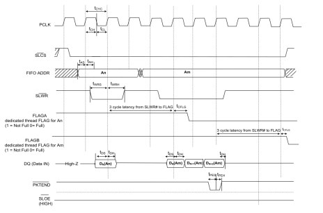
AN65974 The operation is specified in the document GPIF II Interface timing parameters , The screenshot is as follows , Figure 1 shows the synchronous slave device reading sequence , Figure 2 shows the synchronous slave device write sequence , chart 3 It's synchronization ZLP Write cycle timing , chart 4 Is the specific parameter value . It should be noted , This is a Cyusb3014 Timing requirements of the chip , It has nothing to do with what the external controller is . In addition, pay attention to ,PCLK The signal is transmitted by the external controller to Cyusb3014 The clock of , Not its own . You can see , In addition to describing timing parameters, these diagrams , It also points out the sequence of read and write operations , This article will be analyzed as a separate section later .
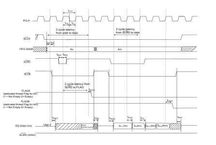
chart 1 Synchronize the sequence read from the device
边栏推荐
- USB(十四)2022-04-12
- Coreseek:第二步建索引及測试
- POJ2392 SpaceElevator [DP]
- Cloud native is devouring everything. How should developers deal with it?
- Ros2 topic (03): the difference between ros1 and ros2 [02]
- Explain
- 在软件工程领域,搞科研的这十年!
- The text editor of markdown class should add colors to fonts (including typora, CSDN, etc.)
- Network security - phishing
- Kubernetes' simplified data storage storageclass (creation, deletion and initial use)
猜你喜欢
JMeter interface automated test read case, execute and write back result

三问TDM
Wechat forum exchange applet system graduation design (5) assignment
![[microservices SCG] gateway integration Sentinel](/img/f3/410d7228b4b253ebf41015a785099f.png)
[microservices SCG] gateway integration Sentinel
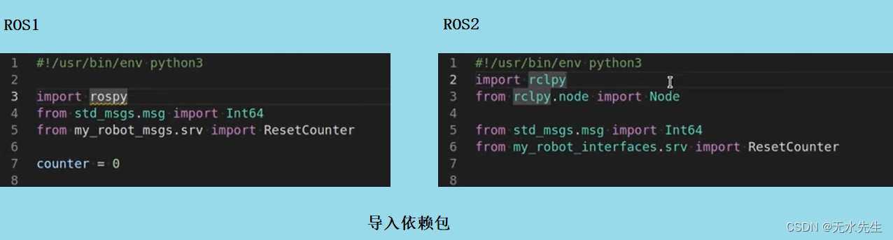
ROS2专题(03):ROS1和ROS2的区别【01】
13、 System optimization
2021icpc Shanghai h.life is a game Kruskal reconstruction tree

Inftnews | the wide application of NFT technology and its existing problems
Cloud native is devouring everything. How should developers deal with it?
JS get the key and value of the object
随机推荐
14、 Two methods of database export and import
The 19th Zhejiang Provincial College Programming Contest 2022 f.easyfix chairman tree
Mysql索引优化实战一
POJ2392 SpaceElevator [DP]
Gee (III): calculate the correlation coefficient between two bands and the corresponding p value
UE4_UE5蓝图command节点的使用(开启关闭屏幕响应-log-发布全屏显示)
The 19th Zhejiang Provincial Collegiate Programming Contest 2022浙江省赛 F.EasyFix 主席树
云原生正在吞噬一切,开发者该如何应对?
成年人只有一份主业是要付出代价的,被人事劝退后,我哭了一整晚
Technology at home and abroad people "see" the future of audio and video technology
ArcGIS: field assignment_ The attribute table field calculator assigns values to fields based on conditions
Redhat下安装fedora
Unity3d learning notes 5 - create sub mesh
Oracle database backup and recovery
Ros2 topic (03): the difference between ros1 and ros2 [01]
Description of longitude and latitude PLT file format
欢聚时代一面
给出一个数组,如 [7864, 284, 347, 7732, 8498],现在需要将数组中的数字拼接起来,返回「最大的可能拼出的数字」
MATLAB signal processing [Q & A essays · 2]
Network security CSRF