当前位置:网站首页>1. Mx6u learning notes (VII): bare metal development (4) -- master frequency and clock configuration
1. Mx6u learning notes (VII): bare metal development (4) -- master frequency and clock configuration
2022-07-06 10:44:00 【A Jiang who gradually loses his hair】
Purpose : Know how to configure the system clock and other peripheral clocks , Make its working frequency 528MHZ, Other peripheral clock sources work in NXP Recommended frequency .
One 、 System clock source
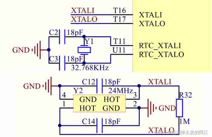
The system clock of the development board comes from two parts :
1、32.768KHZ Crystal oscillator is I.MX6U Of RTC Clock source .
2、24MHZ Crystal oscillator is I.MX6U Clock sources for the kernel and other peripherals .
Two 、7 road PLL Clock source
I.MX6U There are many peripherals , Different peripheral clock sources ,NXP Divide the clock sources of these peripherals into 7 Group , this 7 Group clock sources are from 24MHZ Crystal oscillator PLL And here comes , So it's also called 7 Group PLL. this 7 Group PLL The structure is as follows: :

1、ARM_PLL(PLL1): This road PLL for ARM The kernel using , this PLL By programming, the frequency can be doubled up to 1.3GHZ.
2、528_PLL(PLL2): This road PLL Also called System_PLL, Is constant 22 frequency doubling , Non programmable modification . This road PLL The clock =24MHZ*22=528MHZ. this PLL Separate out 4 road PFD, Respectively :PLL2_PFD0~PLL2_PFD3, this 4 road PFD and 528_PLL As the root clock source of many other peripherals , Usually I.MX6U Clock source of internal system bus , For example, internal processing logic unit 、DDR Interface 、NAND\NOR Interface, etc. .
3、USB1_PLL(PLL3): This road PLL Is constant 20 frequency doubling , therefore USB1_PLL=24MHZ*20=480MHZ. this PLL Also separate 4 road PFD, Respectively :PLL3_PFD0~PLL3_PFD3. This road PLL It is mainly used for USBPHY, But its and four-way PFD It can also be used as the root clock source of other peripherals .
4、USB2_PLL(PLL7): This road PLL Is constant 22 frequency doubling , So it's also 480MHZ. This road PLL It's for USB2PHY The use of .
5、ENET_PLL(PLL6): This road PLL Is constant 20+5/6 frequency doubling , therefore ENET_PLL=500MHZ. This road PLL Used to generate the clock required by the network , Can be here PLL Based on 25/50/100/125MHZ Network clock .
6、VIDEO_PLL(PLL5): This road PLL The output range of is 650MHZ~1300MHZ. This road PLL Used to display related peripherals , such as LCD. This road PLL It can also be done at the time of final output 1/2/4/8/16 frequency division .
7、AUDIO_PLL(PLL4): This road PLL The output range of is 650MHZ~1300MHZ. This road PLL For audio related peripherals . This road PLL It can also be done at the time of final output 1/2/4 frequency division .
3、 ... and 、 Introduction to clock tree

I.MX6U The clock tree is shown in the figure , There are three parts :
1、CLOCK_SWITCHER: namely 7 road PLL and 8 road PFD.
2、CLOCK_ROOT_GENERATOR: In charge of from 7 road PLL and 8 road PFD Select the appropriate clock source for peripherals .
3、SYSTEM_CLOCKS: That is, chip peripherals .

With ESAI Take this peripheral as an example , As shown in the figure, it is divided into 3 part :
1、 This part is the clock source selector ,ESAI There are four optional clock sources :PLL4、PLL5、PLL3_PFD2 and pll3_sw_clk. Specifically choose which way to go ESAI The clock source of , By register CCM->CSCMR2 Of ESAI_CLK_SEL It's up to you .

2、 This part is ESAI Front stage frequency division of clock , The frequency division value is determined by the register CCM_CS1CDR Of ESAI_CLK_PRED To make sure , Can be set up 1~8 frequency division .
3、 This part is also a frequency divider , Further divide the clock output in the second part , The frequency division value is determined by the register CCM_CS1CDR Of ESAI_CLK_PODF To make sure , Can be set up 1~8 frequency division .
Other peripherals and ESAI similar .
Four 、 Kernel clock settings
ARM The kernel clock tree is shown in the figure :

The parts are as follows :
1、 The kernel clock comes from PLL1.
2、 Through registers CCM_CACRR Of ARM_PODF You are right PLL1 Frequency division , Can choose 1/2/4/8 frequency division .
3、 Don't be fooled by this part , It didn't go on 2 frequency division .
4、 After the second step of frequency division, it is ARM Kernel clock , That is to say I.MX6U The main frequency of .
PLL1 The frequency of can be through the register CCM_ANALOG_PLL_ARMn To set up .
register CCM_CACRR Of ARM_PODF Bit can be right PLL1 Divide the frequency of .
CCM_CACRR The register structure is shown in figure :

register CCM_CACRR Only ARM_PODF position , It can be set to 0~7, They correspond to each other 1~8 frequency division .
CCM_ANALOG_PLL_ARMn The register structure is shown in figure :

register CCM_ANALOG_PLL_ARMn The median importance is as follows :
1、ENABLE: Clock output enable bit , Set to 1 Can make PLL1 Output , Set to 0 Just shut it down .
2、DIV_SELECT: This bit is set to PLL1 The output frequency of ,Fout=Fin*div_select/2,Fin=24MHZ. If PLL1 To export 1056MHZ,div_select Just set it to 88.
In the revision PLL1 You need to change the kernel clock source to another clock source before you change the clock frequency ,PLL1 The selectable clock source is shown in the figure :

1、pll_sw_clk Namely PLL1 The final output frequency of .
2、 Here is a selector , choice pll1_sw_clk The clock source of , By register CCM_CCSR Of PLL1_SW_CLK_SEL Bit decision is choice pll1_main_clk still step_clk. Under normal circumstances, you should choose pll1_main_clk, But if you want to be right pll1_main_clk(PLL1) If you adjust the frequency of , For example, to set PLL1=1056MHZ, At this point, we must first pll1_sw_clk Switch to step_clk On , etc. pll1_main_clk Cut back after adjustment .
3、 Here is also a selector , choice step_clk The clock source of , By register CCM_CCSR Of STEP_SEL Bit to decide the choice osc_clk still secondary_clk. General choice osc_clk, That is to say 24MHZ.
register CCM_CCSR Structure is shown in figure :

modify I.MX6U The main frequency steps are as follows :
1、 Set register CCSR Of STEP_SEL position , Set up step_clk The clock source of is 24M The crystal of .
2、 Set register CCSR Of PLL1_SW_CLK_SEL position , Set up pll1_sw_clk The clock source of is step_clk=24MHZ.
3、 Set register CCM_ANALOG_PLL_ARMn, take pll1_main_clk(PLL1) Set to 1056MHZ.
4、 Set register CCSR Of PLL1_SW_CLK_SEL position , Re pll1_sw_clk Switch the clock source back to pll1_main_clk, After switching back pll1_sw_clk Is equal to 1056MHZ.
5、 Finally, set the register CCM_CACRR Of ARM_PODF by 2 frequency division ,I.MX6U The dominant frequency of the kernel is 1056/2=528MHZ.
5、 ... and 、PFD The clock is set
PLL1 It's set up ,PLL2、PLL3 and PLL7 Fixed for 528MHZ、480MHZ and 480MHZ,PLL4~PLL6 All for special peripherals , Set it when you use it . The key is to set PLL2 and PLL3 Their respective 4 road PFD.
NXP The recommended 8 road PFD The frequency is shown in table :
| PFD | NXP Recommended frequency value |
| PLL2_PFD0 | 352MHZ |
| PLL2_PFD1 | 594MHZ |
| PLL2_PFD2 | 400MHZ( For the actual 396MHZ) |
| PLL2_PFD3 | 297MHZ |
| PLL3_PFD0 | 720MHZ |
| PLL3_PFD1 | 540MHZ |
| PLL3_PFD2 | 508.2MHZ |
| PLL3_PFD3 | 454.7MHZ |
First set up PLL2 Of 4 road PFD frequency , register CCM_ANALOG_PFD_528n Structure is shown in figure :

register CCM_ANALOG_PFD_528n Divided into four groups , They correspond to each other PFD0~PFD3, Each group 8 individual bit. How to set PLL2_PFD0 Take the frequency of ,PFD0 The corresponding register bits are as follows :
1、PFD0_FRAC:PLL2_PFD0 Number of frequency divisions ,PLL2_PFD0 The calculation formula of is 528*18/PFD0_FRAC, The setting range of this bit is 12~35.
2、PFD0_STABLE: This bit is read-only , You can judge by reading this bit PLL2_PFD0 Is stable .
3、PFD0_CLKGATE:PLL2_PFD0 Output enable bit , by 1 Turn off , by 0 Time enabled .
If you want to set PLL2_PFD0 The frequency of is 352MHZ, You need to set PFD0_FRAC by 27,PFD0_CLKGATE by 0.PFD1_FRAC=16,PFD2_FRAC=24,PFD3_FRAC=32.
Next set up PLL3_PFD0~PLL3_PFD3 Four way PFD frequency , register CCM_ANALOG_PFD_480n Structure is shown in figure :

The frequency calculation formula is : PLL3_PFDX=480*18/PFDX_FRAC(X=0~3).PFD0_FRAC=12,PFD1_FRAC=16,PFD2_FRAC=17,PFD3_FRAC=19.
6、 ... and 、AHB、IPG and PERCLK Root clock setting
7 road PLL and 8 road PFD After setting, you need to set AHB_CLK_ROOT、IPG_CLK_ROOT and PERCLK_CLK_ROOT The clock of .
I.MX6U The setting range of peripheral root clock is shown in the figure :

AHB_CLK_ROOT and IPG_CLK_ROOT The design of is shown in the figure :

The part divided in the figure :
1、 This selector is used to select pre_periph_clk The clock source of , You can choose PLL2、PLL2_PFD2、PLL2_PFD0 and PLL2_PFD2/2. register CCM_CBCMR Of PRE_PERIPH_CLK_SEL The bit decides which one to choose , Default choice PLL2_PFD2, therefore pre_periph_clk=PLL2_PFD2=396MHZ.
2、 This selector is used to select periph_clk The clock source of , By register CCM_CBCDR Of PERIPH_CLK_SEL Bit and PLL_bypass_en2 Consisting of or to choose from . When CCM_CBCDR Of PERIPH_CLK_SEL Position as 0 when ,periph_clk=pr_periph_clk=396MHZ.
3、 adopt CBCDR Of AHB_PODF Bit to set AHB_CLK_ROOT Frequency division value of , You can set 1~8 frequency division . If you want AHB_CLK_ROOT=132MHZ It should be set to 3 frequency division . Although what is written in the figure is the default 4 frequency division , however I.MX6U Internal boot rom Change it to 3 frequency division .
4、 adopt CBCDR Of IPG_PODF Bit to set IPG_CLK_ROOT Frequency division value of , You can set 1~4 frequency division ,IPG_CLK_ROOT The clock source is AHB_CLK_ROOT, If you want to IPG_CLK_ROOT=66MHZ It should be set up 2 frequency division .
PERCLK_CLK_ROOT The clock structure is shown in the figure :

PERCLK_CLK_ROOT There are two sources :OSC(24MHZ) and IPG_CLK_ROOT, By register CCM_CSCMR1 Of PERCLK_CLK_SEL It's up to you , If 0 Words ,PERCLK_CLK_ROOT The clock source is IPG_CLK_ROOT=66MHZ. It can be done through registers CCM_CSCMR1 Of PERCLK_PODE Bit to set the frequency division .
CCM_CBCDR The register structure is shown in figure :

register CCM_CBCDR The meaning of each bit is as follows :
1、PERIPH_CLK2_PODF:periph2 The clock frequency division , Can be set up 0~7, They correspond to each other 1~8 frequency division .
2、PERIPH2_CLK_SEL: choice peripheral2 The master clock of , If 0 choice PLL2, If 1 choice periph2_clk2_clk. Modifying this bit will cause a connection with MMDC The handshake , So after the modification, wait for the handshake to complete , The handshake completion signal is generated by the register CCM_CDHIPR Middle finger positioning indicates .
3、PERIPH_CLK_SEL: choice peripheral The master clock of , If 0 choice PLL2, If 1 choice periph_clk2_clk. Modifying this bit will cause a connection with MMDC The handshake , So after the modification, wait for the handshake to complete , The handshake completion signal is generated by the register CCM_CDHIPR Middle finger positioning indicates .
4、AXI_PODF:axi The clock frequency division , Can be set up 0~7, They correspond to each other 1~8 frequency division .
5、AHB_PODF:ahb The clock frequency division , Can be set up 0~7, They correspond to each other 1~8 frequency division . Modifying this bit will cause a connection with MMDC The handshake , So after the modification, wait for the handshake to complete , The handshake completion signal is generated by the register CCM_CDHIPR Middle finger positioning indicates .
6、IPG_PODF:ipg The clock frequency division , Can be set up 0~3, They correspond to each other 1~4 frequency division .
7、AXI_ALT_CLK_SEL:axi_alt Clock selection , by 0 Word choice PLL2_PFD2, by 1 Word choice PLL3_PFD1
8、AXI_CLK_SEL:axi Clock source selection , by 0 Word choice periph_clk, by 1 Word choice axi_alt The clock .
9、FABRIC_MMDC_PODF:fabric/mmdc Clock frequency division setting , Can be set up 0~7, They correspond to each other 1~8 frequency division .
10、PERIPH2_CLK2_PODF:periph2_clk2 Clock frequency division of , Can be set up 0~7, They correspond to each other 1~8 frequency division .
CCM_CBCMR The register structure is shown in figure :

register CCM_CBCMR The meaning of each bit is as follows :
1、LCDIF1_PODF:lcdif1 Clock frequency division of , Can be set up 0~7, They correspond to each other 1~8 frequency division .
2、PRE_PERIPH2_CLK_SEL:pre_periph2 Clock source selection ,00 choice PLL2,01 choice PLL2_PFD2,10 choice PLL2_PFD0,11 choice PLL4.
3、PERIPH2_CLK2_SEL:periph2_clk2 Clock source selection , by 0 choice pll3_sw_clk, by 1 choice OSC.
4、PRE_PERIPH_CLK_SEL:pre_periph Clock source selection ,00 choice PLL2,01 choice PLL2_PFD2,10 choice PLL2_PFD0,11 choice PLL2_PFD2/2.
5、PERIPH_CLK2_SEL:peripheral_clk2 Clock source selection ,00 choice pll3_sw_clk,01 choice osc_clk,10 choice pll2_bypass_clk.
CCM_CSCMR1 The register structure is shown in figure :

This register is mainly used for the selection of peripheral clock source , such as QSPI1、ACLK、GPMI、BCH And other peripherals , Focus on the following two :
1、PERCLK_CK_SEL:perclk Clock source selection , by 0 choice ipg_clk, by 1 choice osc_clk.
2、PERCLK_PODF:perclk Clock frequency division of , Can be set up 0~7, They correspond to each other 1~8 frequency division .
When modifying the following clock selector or distributor, it will cause MMDC The handshake happened :
1、MMDC_PODF
2、PERIPH_CLK_SEL
3、PERIPH2_CLK_SEL
4、ARM_PODF
5、AHB_PODF
After the handshake signal occurs, you need to wait for the handshake to complete , register CCM_CDHIPR Whether the handshake signal is completed is stored in the , The corresponding bit is 1 Indicates that it is not completed , by 0 Express completion .
In addition, we are modifying ARM_PODF and AHB_PODF You need to turn off its clock output first , Wait for the modification to complete before opening , Otherwise, there may be a problem that there is no clock output after the modification is completed .
7、 ... and 、 Programming
/* Can make I.MX6U All peripheral clocks */
void clk_enable(void)
{
	CCM->CCGR0 = 0XFFFFFFFF;
	CCM->CCGR1 = 0XFFFFFFFF;
	CCM->CCGR2 = 0XFFFFFFFF;
	CCM->CCGR3 = 0XFFFFFFFF;
	CCM->CCGR4 = 0XFFFFFFFF;
	CCM->CCGR5 = 0XFFFFFFFF;
	CCM->CCGR6 = 0XFFFFFFFF;
}

/* Initialize the system clock , Set the system clock to 792Mhz, And set up PLL2 and PLL3 each PFD The clock , All clock frequencies follow I.MX6U The value recommended by the official manual .*/
void imx6u_clkinit(void)
{
	unsigned int reg = 0;
	/* 1、 Set up ARM The kernel clock is 528MHz */
	if((((CCM->CCSR) >> 2) & 0x1 ) == 0) 	/*  At present pll1_sw_clk The use of pll1_main_clk*/
	{
		CCM->CCSR &= ~(1 << 8);	/*  To configure step_clk The clock source is 24MH OSC */
		CCM->CCSR |= (1 << 2);	/*  To configure pll1_sw_clk The clock source is step_clk */
	}
	CCM_ANALOG->PLL_ARM = (1 << 13) | ((88 << 0) & 0X7F); /*  To configure pll1_main_clk=1056MHz */
	CCM->CCSR &= ~(1 << 2);				/*  take pll_sw_clk The clock switches back to pll1_main_clk */
	CCM->CACRR = 1;					/* ARM The kernel clock is pll1_sw_clk/1=1056/2=528Mhz */

	/* 2、 Set up PLL2(SYS PLL) each PFD */
	reg = CCM_ANALOG->PFD_528;
	reg &= ~(0X3F3F3F3F);		/*  Clear the original settings */
	reg |= 32<<24;			/* PLL2_PFD3=528*18/32=297Mhz */
	reg |= 24<<16;			/* PLL2_PFD2=528*18/24=396Mhz(DDR The clock used , Maximum 400Mhz) */
	reg |= 16<<8;			/* PLL2_PFD1=528*18/16=594Mhz */
	reg |= 27<<0;			/* PLL2_PFD0=528*18/27=352Mhz */
	CCM_ANALOG->PFD_528=reg;	/*  Set up PLL2_PFD0~3*/

	/* 3、 Set up PLL3(USB1) each PFD */
	reg = 0;				/*  Zero clearing */
	reg = CCM_ANALOG->PFD_480;
	reg &= ~(0X3F3F3F3F);		/*  Clear the original settings */
	reg |= 19<<24;			/* PLL3_PFD3=480*18/19=454.74Mhz */
	reg |= 17<<16;			/* PLL3_PFD2=480*18/17=508.24Mhz */
	reg |= 16<<8;			/* PLL3_PFD1=480*18/16=540Mhz*/
	reg |= 12<<0;			/* PLL3_PFD0=480*18/12=720Mhz*/
	CCM_ANALOG->PFD_480=reg;	/*  Set up PLL3_PFD0~3 */

	/* 4、 Set up AHB The clock is the smallest 6Mhz,  Maximum 132Mhz (boot rom It can be set automatically without setting )*/
	CCM->CBCMR &= ~(3 << 18); 	/*  Clear settings */
	CCM->CBCMR |= (1 << 18);		/* pre_periph_clk=PLL2_PFD2=396MHz */
	CCM->CBCDR &= ~(1 << 25);	/* periph_clk=pre_periph_clk=396MHz */
	while(CCM->CDHIPR & (1 << 5));	/*  Wait for the handshake to complete  */


	/* 5、 Set up IPG_CLK_ROOT Minimum 3Mhz, Maximum 66Mhz (boot rom It can be set automatically without setting )*/
	CCM->CBCDR &= ~(3 << 8);	/* CBCDR Of IPG_PODF Zero clearing  */
	CCM->CBCDR |= 1 << 8;	/* IPG_PODF 2 frequency division ,IPG_CLK_ROOT=66MHz */

	/* 6、 Set up PERCLK_CLK_ROOT The clock  */
	CCM->CSCMR1 &= ~(1 << 6);/* PERCLK_CLK_ROOT The clock source is IPG */
	CCM->CSCMR1 &= ~(7 << 0);/* PERCLK_PODF A reset , namely 1 frequency division  */
}
边栏推荐
- Typescript入门教程(B站黑马程序员)
- Mysql30 transaction Basics
- IDEA 导入导出 settings 设置文件
- ① BOKE
- Breadth first search rotten orange
- How to find the number of daffodils with simple and rough methods in C language
- Baidu Encyclopedia data crawling and content classification and recognition
- MySQL35-主从复制
- 用于实时端到端文本识别的自适应Bezier曲线网络
- Set shell script execution error to exit automatically
猜你喜欢
MySQL 20 MySQL data directory
Mysql35 master slave replication
MySQL23-存儲引擎
Typescript入门教程(B站黑马程序员)
A brief introduction to the microservice technology stack, the introduction and use of Eureka and ribbon

ByteTrack: Multi-Object Tracking by Associating Every Detection Box 论文阅读笔记()
Mysql36 database backup and recovery

Moteur de stockage mysql23
MySQL 29 other database tuning strategies

Mysql25 index creation and design principles
随机推荐
API learning of OpenGL (2004) gl_ TEXTURE_ MIN_ FILTER GL_ TEXTURE_ MAG_ FILTER
UEditor国际化配置,支持中英文切换
Installation and use of MySQL under MySQL 19 Linux
Bytetrack: multi object tracking by associating every detection box paper reading notes ()
CSDN问答标签技能树(一) —— 基本框架的构建
Implement sending post request with form data parameter
Use of dataset of pytorch
Moteur de stockage mysql23
What is the current situation of the game industry in the Internet world?
Navicat 导出表生成PDM文件
MySQL21-用户与权限管理
35 is not a stumbling block in the career of programmers
CSDN Q & a tag skill tree (V) -- cloud native skill tree
Technology | diverse substrate formats
MySQL35-主从复制
MySQL23-存储引擎
API learning of OpenGL (2001) gltexgen
Windchill configure remote Oracle database connection
npm一个错误 npm ERR code ENOENT npm ERR syscall open
Not registered via @enableconfigurationproperties, marked (@configurationproperties use)