当前位置:网站首页>Verilog realizes nixie tube display driver [with source code]
Verilog realizes nixie tube display driver [with source code]
2022-07-07 11:15:00 【Lime Miya】
Catalog
1、 The experiment platform
 Software :PC、Quartus Prime 18.1、Modelsim 10.5b
 Hardware :Altera FPGA Development board (EP4CE6E22F17C8)
2、 The experiment purpose
- 1、 Master the static display and dynamic refresh of nixie tube
- 2、 Counter exercise
2.1、 Experimental content
 Static display  0~F
 Dynamic display - Stopwatch design
3、 Experimental process
3.1、 Experimental principle
According to the schematic diagram of the development board , The following information is available
Nixie tube : It is essentially a group of light-emitting diodes arranged in a certain order , Its display principle and LED It's no different .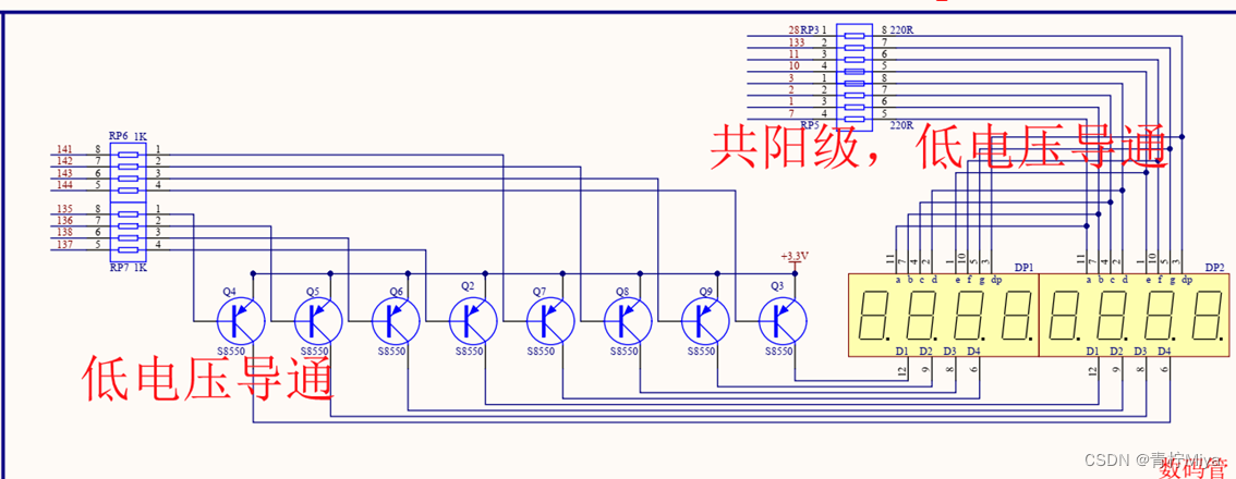
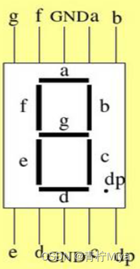
 According to the hardware schematic diagram , Light-emitting diode , All anodes are switched on 3.3V Positive voltage of , That is to say — High level , So if we want to
 If the LED is on , It is necessary to turn on the low level at the cathode , You can make LED Light up .
3.2、 System architecture
According to the system requirements , The following frame distribution can be obtained
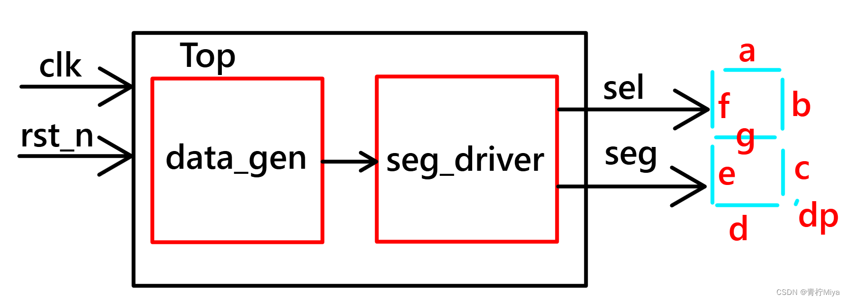
3.3、 Function module division
Build according to the system , The following modules are available
3.3.1、 Data generation module
Block diagram
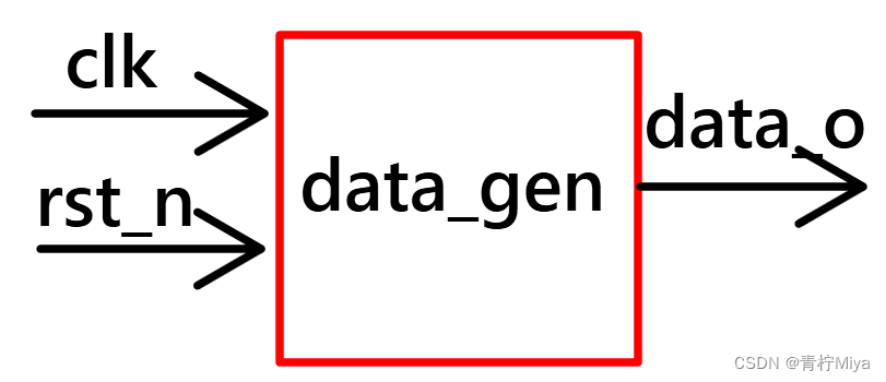
Signal definition
| Signal name | Port type | Data bit width | Signal description |
|---|---|---|---|
| Clk | i | 1 | Input clock signal ,50MHz |
| Rst_n | i | 1 | Input reset signal , Low level active |
| data_o | O | 32 | Output data to be displayed ,8 Digit nixie tube can display 32 position 16 Hexadecimal data |
Design documents
/*================================================*\ Filename ﹕data_gen.v Author ﹕Adolph Description ﹕ Generate the data that the nixie tube needs to display . 32'h11111111~32'h33333333; Called by ﹕seg_top.v Revision History ﹕ 2022-6-6 15:49:24 Revision 1.0 Email﹕[email protected] Company﹕ \*================================================*/
module data_gen(
	input	clk	,
	input	rst_n,

	output	reg [31:0] data_dis
);

	parameter TIME_DELAY = 25'd2500;

	reg		[24:0]	cnt_delay;

	[email protected](posedge clk or negedge rst_n)begin
		if(!rst_n)begin
			cnt_delay <= 25'd0;
		end
		else if(cnt_delay >= TIME_DELAY - 25'd1)begin
			cnt_delay <= 25'd0;
		end
		else begin
			cnt_delay <= cnt_delay + 25'd1;
		end
	end

	[email protected](posedge clk or negedge rst_n)begin
		if(!rst_n)begin
			data_dis <= 32'h1111_1111;
		end
		else if(data_dis == 32'h3333_3333)begin
			data_dis <= 32'h1111_1111;
		end
		else if(cnt_delay >= TIME_DELAY - 25'd1)begin
			data_dis <= data_dis + 32'h1;
		end
		else begin
			data_dis <= data_dis;
		end
	end

endmodule
This module is relatively simple , Simulation verification is not done here , If you are interested, you can verify by yourself
3.3.2、 Digital tube driver module
Block diagram
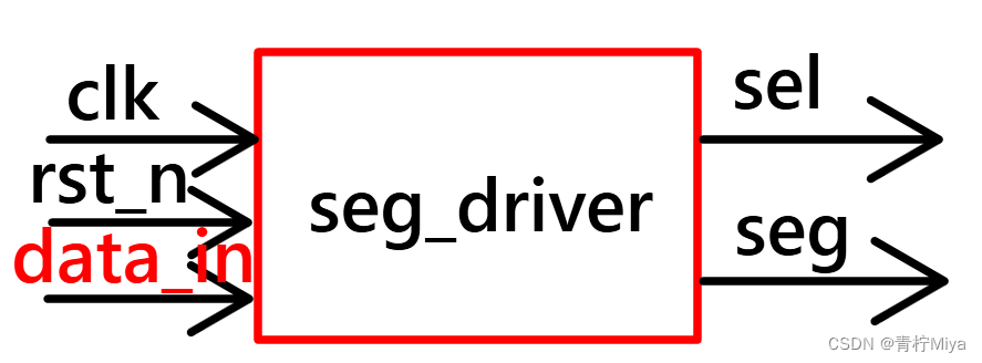
Signal definition
| Signal name | Port type | Data bit width | Signal description |
|---|---|---|---|
| Clk | i | 1 | Input clock signal ,50MHz |
| Rst_n | i | 1 | Input reset signal , Low level active |
| data_in | i | 32 | Input the key debounce signal , High active |
| dig_sel | O | 8 | Digital tube position selection signal , It can be seen from the schematic diagram that , Low level active |
| dig_seg | O | 8 | Select the signal section , It can be seen from the schematic diagram that , Low level active |
Design documents
/*================================================*\ Filename ﹕seg_driver.v Author ﹕Adolph Description ﹕ Decode the input data , And drive the nixie tube to display the corresponding data  Called by ﹕seg_top.v Revision History ﹕ 2022-5-30 14:27:22 Revision 1.0 Email﹕[email protected] Company﹕ \*================================================*/
module seg_driver(
	input			clk		,
	input			rst_n	,

	input	  [31:0]dis_data,// Data to be displayed
	output reg[7:0]	dig_sel	,
	output reg[7:0]	dig_seg
);
//wire [31:0]dis_data;


// assign dig_seg = 8'd0;
// assign dig_sel = 1'b0;
	localparam
		NUM_0  	= 8'hC0,
		NUM_1  	= 8'hF9,
		NUM_2  	= 8'hA4,
		NUM_3  	= 8'hB0,
		NUM_4  	= 8'h99,
		NUM_5  	= 8'h92,
		NUM_6  	= 8'h82,
		NUM_7  	= 8'hF8,
		NUM_8  	= 8'h80,
		NUM_9  	= 8'h90,
		NUM_A  	= 8'h88,
		NUM_B  	= 8'h83,
		NUM_C  	= 8'hC6,
		NUM_D  	= 8'hA1,
		NUM_E  	= 8'h86,
		NUM_F  	= 8'h8E,
		LIT_ALL	= 8'h00,
		BLC_ALL	= 8'hFF;
	parameter CNT_REF = 25'd1000;

	reg	[9:0]	cnt_20us; //20us Counter
	reg	[3:0] 	data_tmp; // It is used to get the display data of different bit selections

// assign dis_data = 32'hABCD_4413;
// Describe bit selection signal switching
	// Description refresh counter
	[email protected](posedge clk or negedge rst_n)begin
		if(!rst_n)begin
			cnt_20us <= 25'd0;
		end
		else if(cnt_20us >= CNT_REF - 25'd1)begin
			cnt_20us <= 25'd0;
		end
		else begin
			cnt_20us <= cnt_20us + 25'd1;
		end
	end

	[email protected](posedge clk or negedge rst_n)begin
		if(!rst_n)begin
			dig_sel <= 8'hfe;//8'b1111_1110
		end
		else if(cnt_20us >= CNT_REF - 25'd1)begin
			dig_sel <= {
    dig_sel[6:0],dig_sel[7]};
		end
		else begin
			dig_sel <= dig_sel;
		end
	end

// Segment selection signal description
	[email protected](posedge clk or negedge rst_n)begin
		if(!rst_n)begin
			data_tmp <= 4'd0;
		end
		else begin
			case(dig_sel)
				8'b1111_1110:data_tmp <= dis_data[ 3-:4];
				8'b1111_1101:data_tmp <= dis_data[ 7-:4];
				8'b1111_1011:data_tmp <= dis_data[11-:4];
				8'b1111_0111:data_tmp <= dis_data[15-:4];
				8'b1110_1111:data_tmp <= dis_data[19-:4];
				8'b1101_1111:data_tmp <= dis_data[23-:4];
				8'b1011_1111:data_tmp <= dis_data[27-:4];
				8'b0111_1111:data_tmp <= dis_data[31-:4];
				default: data_tmp <= 4'hF;
			endcase
		end
	end

	[email protected](posedge clk or negedge rst_n)begin
		if(!rst_n)begin
			dig_seg <= BLC_ALL;
		end
		else begin
			case(data_tmp)
				4'h0 : dig_seg <= NUM_0;
				4'h1 : dig_seg <= NUM_1;
				4'h2 : dig_seg <= NUM_2;
				4'h3 : dig_seg <= NUM_3;
				4'h4 : dig_seg <= NUM_4;
				4'h5 : dig_seg <= NUM_5;
				4'h6 : dig_seg <= NUM_6;
				4'h7 : dig_seg <= NUM_7;
				4'h8 : dig_seg <= NUM_8;
				4'h9 : dig_seg <= NUM_9;
				4'hA : dig_seg <= NUM_A;
				4'hB : dig_seg <= NUM_B;
				4'hC : dig_seg <= NUM_C;
				4'hD : dig_seg <= NUM_D;
				4'hE : dig_seg <= NUM_E;
				4'hF : dig_seg <= NUM_F;
				default: ;
			endcase
		end
	end

endmodule
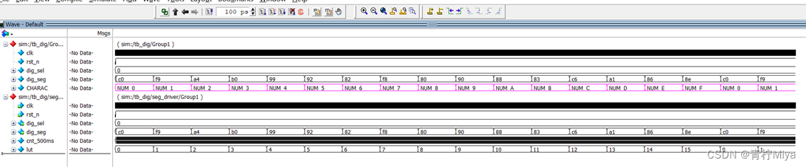
Simulation verification
`timescale 1ns/1ns

module tb_dig;
	reg		clk;
	reg		rst_n;

	wire	[7:0]	dig_sel;
	wire    [7:0]	dig_seg;

	reg		[39:0]	CHARAC;//1 individual  ASCII  code , need 8bit  Binary representation

	defparam seg_driver.CNT_REF = 100;

	localparam
		NUM_0 = 8'hC0,
		NUM_1 = 8'hF9,
		NUM_2 = 8'hA4,
		NUM_3 = 8'hB0,
		NUM_4 = 8'h99,
		NUM_5 = 8'h92,
		NUM_6 = 8'h82,
		NUM_7 = 8'hF8,
		NUM_8 = 8'h80,
		NUM_9 = 8'h90,
		NUM_A = 8'h88,
		NUM_B = 8'h83,
		NUM_C = 8'hC6,
		NUM_D = 8'hA1,
		NUM_E = 8'h86,
		NUM_F = 8'h8E;

	[email protected](*)begin
		case(dig_seg)
			NUM_0 : CHARAC = "NUM_0";
			NUM_1 : CHARAC = "NUM_1";
			NUM_2 : CHARAC = "NUM_2";
			NUM_3 : CHARAC = "NUM_3";
			NUM_4 : CHARAC = "NUM_4";
			NUM_5 : CHARAC = "NUM_5";
			NUM_6 : CHARAC = "NUM_6";
			NUM_7 : CHARAC = "NUM_7";
			NUM_8 : CHARAC = "NUM_8";
			NUM_9 : CHARAC = "NUM_9";
			NUM_A : CHARAC = "NUM_A";
			NUM_B : CHARAC = "NUM_B";
			NUM_C : CHARAC = "NUM_C";
			NUM_D : CHARAC = "NUM_D";
			NUM_E : CHARAC = "NUM_E";
			NUM_F : CHARAC = "NUM_F";
			default : CHARAC = "NUM_0";
		endcase
	end

	seg_driver		seg_driver(
	/*input */.clk		(clk	),
	/*input */.rst_n	(rst_n	),

	/*output reg[7:0] */.dig_sel	(dig_sel),
	/*output reg[7:0] */.dig_seg	(dig_seg)
);

	initial clk = 1'b0;
	always #10 clk = ~clk;

	initial begin
		rst_n = 1'b0;
		#36 rst_n = 1'b1;

		wait (seg_driver.lut == 15);

		#(20 * seg_driver.CNT_REF * 3);

		$stop(2);
	end

endmodule
3.3.3、 Top level documents
The top-level document is not explained here , According to the following RTL View , I believe that readers can easily complete the corresponding code design
RTL View 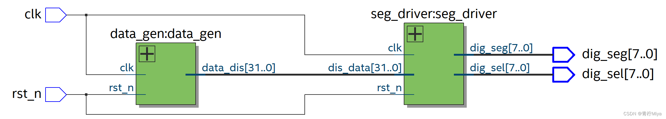
3.4、 Board level verification
You can see that the nixie tube is made of 32‘h11111111 Every time it's self increasing 1, The change rate can be adjusted in the data generation module .
4、 summary
 This design realizes the basic character display , Dynamic scanning
 You can finish the stopwatch based on your own understanding 、 Digital clock design , Believe that smart you can , come on. !
边栏推荐
- Force buckle 1002 Find common characters
- 关于在云服务器上(这里用腾讯云)安装mysql8.0并使本地可以远程连接的方法
- Vuthink proper installation process
- Eth trunk link switching delay is too high
- Avoid mutating a prop directly since the value will be overwritten whenever the parent component
- Ffmpeg record a video command from RTSP
- Poj1821 fence problem solving Report
- Use of dotween
- What if copying is prohibited?
- 90后,辞职创业,说要卷死云数据库
猜你喜欢
Still cannot find RPC dispatcher table failed to connect in virtual KD
基于华为云IOT设计智能称重系统(STM32)
How to remove addition and subtraction from inputnumber input box
Deep understanding of Apache Hudi asynchronous indexing mechanism
Vscode 尝试在目标目录创建文件时发生一个错误:拒绝访问【已解决】
The opacity value becomes 1%
"Dream Cup" 2017 Jiangsu information and future primary school summer camp it expert PK program design questions
Array object sorting
electron添加SQLite数据库
![[untitled]](/img/15/3db921703147afdf58dfffe532a19b.jpg)
[untitled]
随机推荐
[OneNote] can't connect to the network and can't sync the problem
The seventh training assignment
Force buckle 1002 Find common characters
VR development optimization
测试优惠券要怎么写测试用例?
关于jmeter中编写shell脚本json的应用
Array object sorting
IDEA快捷键大全
毕业季|与青春作伴,一起向未来!
Project ERROR: Unknown module(s) in QT: core gui
2021-05-21
Go redis Middleware
What if copying is prohibited?
Interprocess communication (IPC)
面试被问到了解哪些开发模型?看这一篇就够了
After the uniapp jumps to the page in onlaunch, click the event failure solution
【C#】WinForm运行缩放(变糊)的解决方法
Vuthink proper installation process
Hash / (understanding, implementation and application)
2021-04-08