当前位置:网站首页>Tms320c665x + Xilinx artix7 DSP + FPGA high speed core board
Tms320c665x + Xilinx artix7 DSP + FPGA high speed core board
2022-07-06 06:26:00 【Xinmai technology dsp+arm+fpga】
1 Introduction to core board
- be based on TI KeyStone C66x Multicore site / floating-point DSP TMS320C665x + Xilinx Artix-7 FPGA processor ;
- TMS320C665x The main frequency is 1.0G/1.25GHz, Single core computing power is as high as 40G MACS and 20G FLOPS,FPGA XC7A100T Logical unit 101K individual ,DSP Slice 240 individual ;
- TMS320C665x And FPGA adopt uPP、EMIF、I2C、PCIe、SRIO Wait for the communication interface to connect , among PCIe、 SRIO The highest transmission speed of each channel can be achieved 5 GBaud;
- FPGA The acquisition card supports two channels 250MSPS*12Bit High speed and high precision ADC, All the way 175MSPS*12Bit High speed and high precision DAC, Meet a variety of data acquisition needs ;
- Support gigabit network port , It can be connected to an industrial webcam , Support at the same time I2C、SPI、UART、McBSP And other common interfaces ; Ø
- Support CameraLink Input and output 、VGA Output and other expansion modules ;
- Support for bare metal and SYS/BIOS operating system .
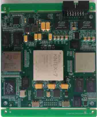
chart 1 Development board
Shenzhen Xinmai is based on TI The design of the XM-C665xF-EVM Is a DSP+FPGA High speed big data acquisition and processing architecture , For high-end image processing 、 High speed big data transmission, audio and video and other big data acquisition and processing fields . This design passes TMS320C665x Of uPP、EMIF、I2C、PCIe、SRIO And other communication interfaces combine the boards and cards together , form DSP+FPGA framework , Achieve unique needs 、 flexible 、 Powerful DSP+FPGA High speed data acquisition and processing system .
SOM-XM665xF extraction CPU All resource signal pins , Secondary development is extremely easy , The customer just needs to focus on the top use , Reduced development difficulty and time cost , Get the product on the market quickly , Seize the market in time . Not only provide abundant
Rich Demo Program , Also provide DSP Development course of inter core communication , Comprehensive technical support , Assist the customer to carry out the inspection
Design and debugging and multi-core software development .
2 Typical applications
- Data acquisition and processing display system Telecom Tower: Remote RF unit (RRU) High speed data acquisition and generation
- High speed data acquisition and processing system
- High end image processing equipment
- High end audio and video data processing
- communication system
3 Software and hardware parameters
- The front end is composed of FPGA Collect two channels AD data ,AD Data is passed through uPP、EMIF Bus or PCIe、SRIO Interface and other communication interfaces are transmitted to DSP. Ø
- AD The data is DSP After processing , It can be used for data comparison and analysis 、 Network forwarding 、SATA Hard disk storage and other applications .
- DSP According to the result , Send the obtained logic control command to FPGA, from FPGA The control board carries DA Realize logic output , Update rate 175MSPS.
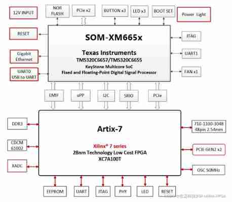
chart 2 Block diagram of big data acquisition principle
- The front-end part of high-speed data acquisition is composed of FPGA Synchronous acquisition of two channels AD Analog input signal , It can be realized to AD Pre filter the data ,AD The highest sampling rate is 250MSPS. The other way DAC It can output parallel signals with arbitrary amplitude and waveform DA data , Update rate 175MSPS.
- The high-speed data transmission part consists of EMIF、I2C、PCIe、SRIO And other communication interfaces . Large throughput AD and DA data , It can be done by SRIO and PCIe Interface in DSP and FPGA High speed and stable transmission between ;DSP It can be done by EMIF Bus pair FPGA Logic control and data exchange with medium throughput , At the same time, it can be done through I2C Yes FPGA Initialization setting and parameter configuration at the end .
(3) The high-speed data processing part consists of DSP Core and algorithm library . It can be realized to AD and DA The data are analyzed in time domain 、 frequency
Domain 、 The amplitude and other signal parameters are transformed in real time ( Such as FFT Transformation 、FIR Filtering, etc ).
(4) Video capture 、 The output expansion part consists of CameraLink I / O module 、VGA output module 、 Gigabit network, etc
Part of the form . Rich interface resources , The scheme selection is flexible and convenient , It is an ideal choice for high-end image processing system .
3.1 Hardware parameters
surface 1 XM6678-EasyEVM Hardware parameters
CPU | Single core TMS320C6655/ Dual core TMS320C6657, Main frequency 1.0/1.25GHz |
ROM | 128/256MByte NAND FLASH |
RAM | 512M/1G Byte DDR3 |
EEPROM | 1Mbit |
FLASH | 32/64Mbit SPI NOR FLASH |
LED | 1x Power supply indicator |
1x Programmable indicator | |
sensor | 1x TMP102, Core board temperature sensor ,I2C Interface |
The connector | 2x 50pin Male head B2B,2x 50pin Female head B2B, spacing 0.8mm, Hegao 5.0mm, common 200pin |
1x 80pin High speed B2B The connector , spacing 0.5mm, Hegao 5.0mm, The signal rate can reach 10GBaud | |
expand IO | 2x 25pin IDC3 Simple bracket , spacing 2.54mm, contain EMIF16 Expansion signal |
2x 25pin IDC3 Simple bracket , spacing 2.54mm, contain SPI、I2C、TIMER、GPIO Wait for the expansion signal | |
2x 25pin IDC3 Simple bracket , spacing 2.54mm, contain TSIP Expansion signal | |
1x SRIO 2.1 TX,1x SRIO 2.1 RX,4 passageway , Maximum communication rate per channel 5GBaud | |
1x PCIe 4x(Gen2),2 passageway , Maximum communication rate per channel 5GBaud | |
1x HyperLink, Maximum communication rate 40GBaud,KeyStone The ideal interface for interconnection between processors | |
Emulator interface | 1x 14pin TI Rev B JTAG Interface , spacing 2.54mm |
Key | 2x Reset button |
1x Unshielded interrupt button | |
1x User programmable keys | |
Starting mode | 1x 5bit Starting mode , Select the dial switch |
The Internet | 2x Ethernet,10/100/1000M The adaptive |
A serial port | 1x UART0,USB To serial port , Provide 4 The needle TTL Level test port |
1x UART1,DB9 Interface , Provide 6 The needle TTL Level test port | |
Fan connector | 1x FAN,12V Power supply , spacing 2.54mm |
power switch | 1x Power dial switch |
The power interface | 1x 12V 3A DC input DC417 The power interface , Outside diameter 4.4mm, The inner diameter 1.65mm |
remarks : Shenzhen Xinmai SOM-XM6655、SOM-XM6657 The core board is on the hardware pin to pin compatible .
surface 2 XM-A7HSAD Hardware parameters
CPU | Xilinx Artix-7 XC7A100T FPGA |
RAM | 256Mbit NOR FLASH |
ROM | 2x 128M/256MByte DDR3 |
EEPROM | 2KBit |
The Internet | 1x Ethernet,10/100/1000M The adaptive |
LED | 2x Power supply indicator |
3x Programmable indicator | |
Key | 2x Reset button |
2x User programmable keys | |
ADC | Two channels ,1.8Vp-p,12bit, The highest 250MHz Sampling rate ,LVDS Signal output |
DAC | 175MHz,12bit, Maximum output current 5mA |
XADC | Two channels ,12bit,1MHz,1.25Vp-p |
expand IO | 1x SRIO TX,1x SRIO RX,4 passageway , Single channel maximum rate 5GBaud,HDMI seat |
1x PCIe 4x(Gen2),2 passageway , Maximum communication rate of single channel 5GBaud | |
2x 48pin European connector ,GPIO expand | |
1x I2C,HDMI seat | |
Emulator interface Starting mode | 1x 14pin JTAG Interface , spacing 2.00mm 1x 2bit Start mode selection dial switch |
A serial port | 1x UART,Micro USB Interface , Provide 4 The needle TTL Level test port |
power switch | 1x Power dial switch |
The power interface | 1x 12V 2A DC input DC005 The power interface , Outside diameter 5.5mm, The inner diameter 2.1mm |
3.2 Software parameters
surface 3
DSP End software support | Bare pager 、SYS/BIOS operating system |
CCS Version number | CCS5.5 |
The software development kit provides | MCSDK |
Vivado Version number | 2015.2 |
4 Development of information
(1) Provide core board pin definition 、 The schematic diagram of the bottom plate can be edited 、 Editable backplane PCB、 chip Datasheet, To shorten the
Hardware design cycle ;
(2) Provide a wealth of Demo Program , contain DSP Multi core communication course , Solve the bottleneck of multi-core development perfectly ;
- Provide DSP And FPGA adopt PCIe、SRIO、I2C And other related communication routines ;
- Provide a complete platform development package 、 Introductory tutorial , Save time in software development , Make application development easier ;
Development cases mainly include : Ø
- Bare metal development routines
- SYS/BIOS Development routines
- Multi core development routines
- FPGA Development routines
5 Electrical characteristics
Core board working environment
Environmental parameters | minimum value | Typical values | Maximum |
Core board operating temperature | -40°C | / | 85°C |
Working voltage of core board | / | 5.0V | / |
Power consumption test
Category | Voltage typical value | Typical value of current | Typical power consumption |
Core board | 9.0v | 390mA | 3.5W |
remarks : The power consumption test is based on Shenzhen Xinmai XM-C665xF-EVM Development board .
6 Mechanical Dimensions
surface 4
Core board | Evaluate the floor | |
PCB Size | 80mm*58mm | 200mm*106.5mm |
Number of fixed mounting holes | 4 | 4 |
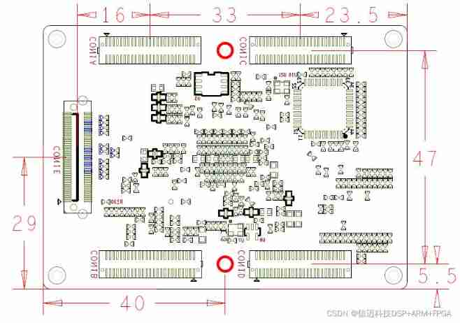
chart 6 Mechanical dimension drawing of core plate
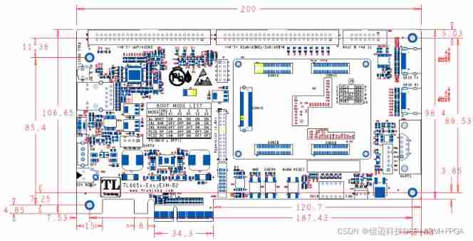
chart 7 Mechanical dimension drawing of evaluation board
7 technical service
- Assist in floor design and testing , Reduce hardware design mistakes ;
- Help to solve the abnormal problems in accordance with the user manual ;
- Assist in product failure determination ;
- Help compile and run the supplied source code correctly ;
- Assist in secondary product development ;
- Provide long-term after-sales service .
8 Value added service
- Motherboard custom design
- Customized design of core board
- Embedded software development
- Project Co development
- Technical training
边栏推荐
- Simulation volume leetcode [general] 1314 Matrix area and
- Simulation volume leetcode [general] 1414 The minimum number of Fibonacci numbers with a sum of K
- [C language] qsort function
- Simulation volume leetcode [general] 1249 Remove invalid parentheses
- Simulation volume leetcode [general] 1405 Longest happy string
- Oscp raven2 target penetration process
- oscp raven2靶机渗透过程
- Digital triangle model acwing 1015 Picking flowers
- Py06 字典 映射 字典嵌套 键不存在测试 键排序
- 如何将flv文件转为mp4文件?一个简单的解决办法
猜你喜欢
私人云盘部署
Error getting a new connection Cause: org. apache. commons. dbcp. SQLNestedException
![[eolink] PC client installation](/img/91/8b3c4264e544b14f926e91edddf18d.png)
[eolink] PC client installation
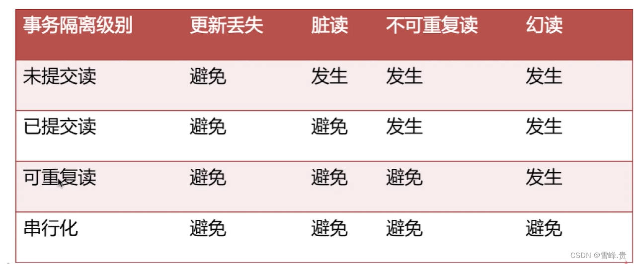
Database isolation level
My daily learning records / learning methods
![[Tera term] black cat takes you to learn TTL script -- serial port automation skill in embedded development](/img/63/dc729d3f483fd6088cfa7b6fb45ccb.png)
[Tera term] black cat takes you to learn TTL script -- serial port automation skill in embedded development
Luogu p2089 roast chicken

翻译公司证件盖章的价格是多少

Career advancement Guide: recommended books for people in big factories
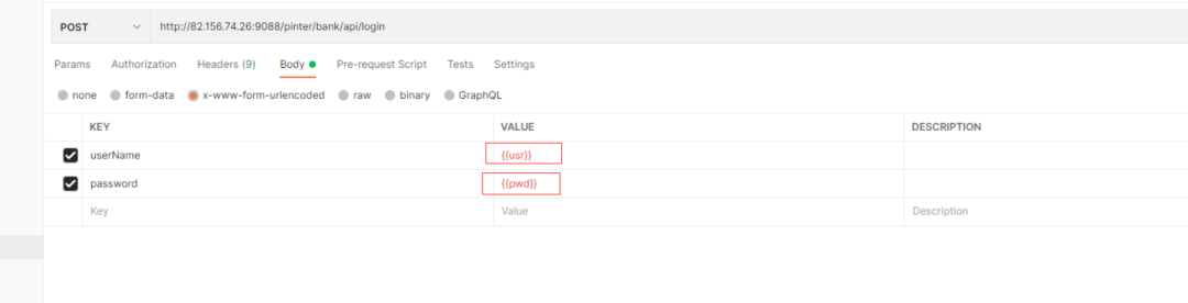
Postman core function analysis - parameterization and test report
随机推荐
Simulation volume leetcode [general] 1414 The minimum number of Fibonacci numbers with a sum of K
模拟卷Leetcode【普通】1143. 最长公共子序列
Transfert des paramètres de la barre d'adresse de la page de liste basée sur jeecg - boot
如何做好互联网金融的英语翻译
Mise en œuvre d’une fonction complexe d’ajout, de suppression et de modification basée sur jeecg - boot
数据库-当前读与快照读
数据库隔离级别
Redis 核心技术与实战之 基本架构:一个键值数据库包含什么?
私人云盘部署
翻译影视剧字幕,这些特点务必要了解
The ECU of 21 Audi q5l 45tfsi brushes is upgraded to master special adjustment, and the horsepower is safely and stably increased to 305 horsepower
Address bar parameter transmission of list page based on jeecg-boot
使用Nacos管理配置
今日夏至 Today‘s summer solstice
Customize the gateway filter factory on the specified route
JWT-JSON WEB TOKEN
联合索引的左匹配原则
Database - current read and snapshot read
E - food chain
leetcode 24. 两两交换链表中的节点