当前位置:网站首页>Working principle of genius telephone watch Z3
Working principle of genius telephone watch Z3
2022-07-06 12:05:00 【FAE Laobing】
1. Z3 Hardware configuration of the whole machine 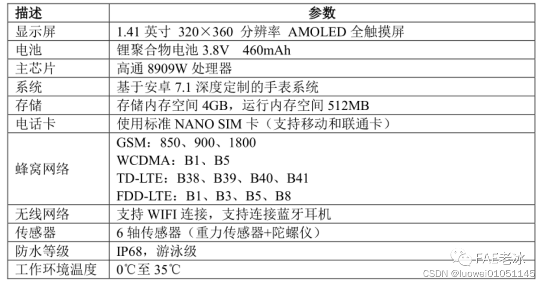
2. Block diagram of complete machine 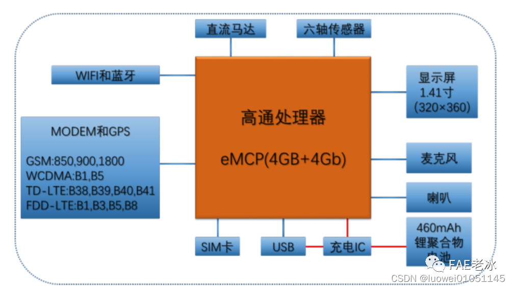
qualcomm MSM8909W use 28 Made by nano technology ARM Cortex A7 Architecture's processor , Can provide 3 G and 4G High speed data processing and rich multimedia functions ; This multimode solution supports the latest air interface standards , Include 1xEV-DorA/1x Advanced/DC-HSPA+/TD-SCDMA and LTE; The highly integrated feature enables it to maintain the functions of mobile devices while reducing the chip space .
3. Motherboard device 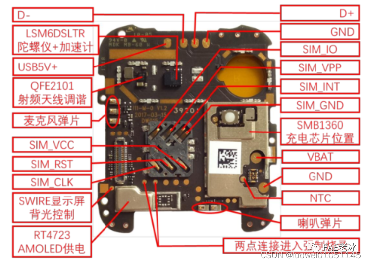
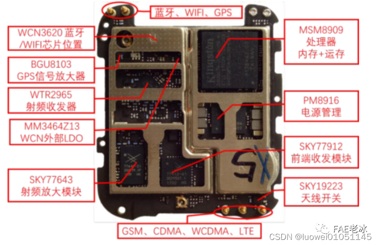
4. working principle
4.1 Power control circuit
4.1.1 Charging chip SMB1360
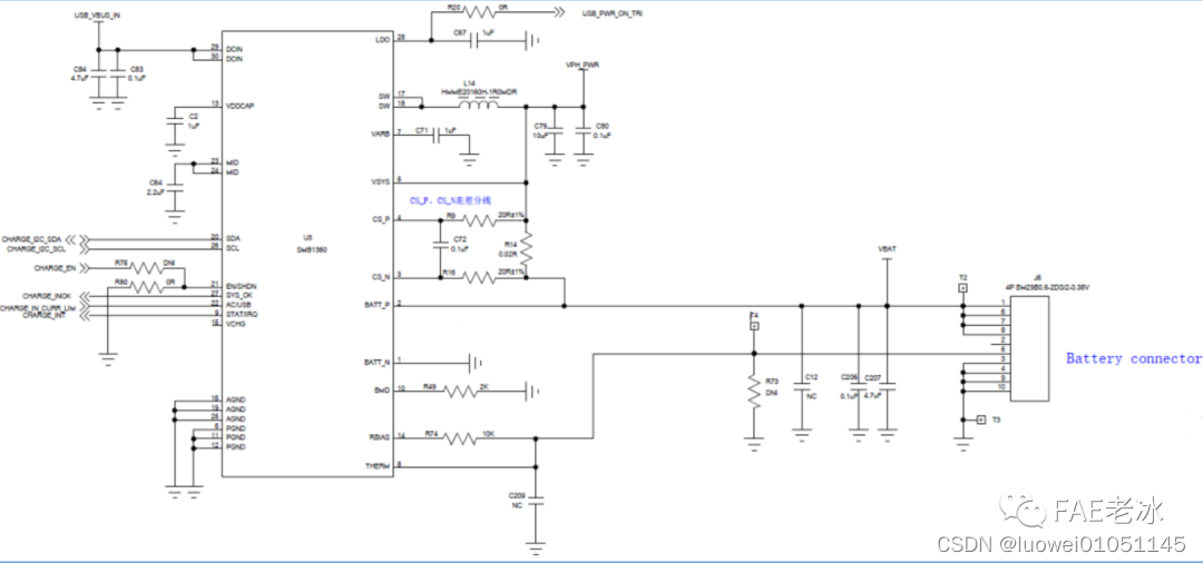
SMB1360 It is a kind of switch programmable lithium ion / Lithium polymer battery charger and high-precision coulometer chip . The device provides a simple and effective way to charge high-capacity lithium-ion batteries , And provide the charging state information of the battery . The switch charger device can detect the maximum AC / The DC adapter stabilizes the output current and automatically adjusts the input current level , This automatically matches the external adapter . The buck converter structure effectively multiplies the input current , To improve the charging rate of lithium-ion batteries . Charging control includes limit values 、 Trickle charging 、 Precharge 、 constant current / Constant voltage charging 、 Floating voltage and termination / Security Settings .
SMB1360 The device also provides battery and charger protection and input circuit protection , If it's over current , Overvoltage and thermal protection . It also provides the function of missing battery detection , To detect the condition of missing battery .STAT The output can be used to provide charging state information to the system . The working temperature is -30℃ To 85℃ between .
4.1.2 Power management PM8916
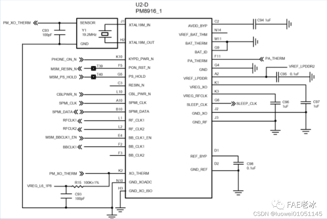
PM8916 Manage the power supply of wireless handheld devices 、 Integrated management and user interface support functions are integrated into a single mixed signal integrated circuit , Its multi-function design is suitable for multi-mode 、 In multiband phones and other wireless products .
U2-D by PM8916 Control and clock management module ,PHONE_ON_N For the switch pin .
U2-E For input / Output (GPIOs) And multi-purpose pins (MPPs) modular .
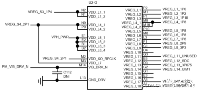
U2-G by PM8916 Of LDOs Circuit module .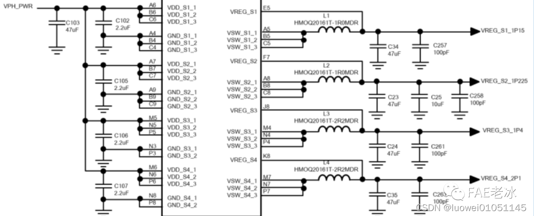
U2-F by PM8916 Switching power supply of (SMPS) Circuit part .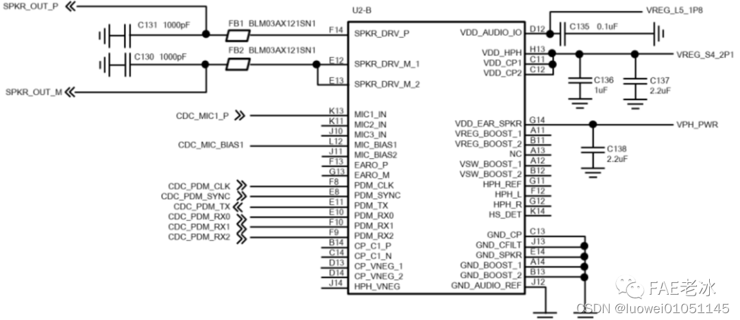
U2-B by PM8916 The audio processing module of .
4.1.3 The display shows the power supply chip
RT4723WSC It is a display screen that shows the power supply chip , Negative output voltage can pass SWIRE The interface protocol is from -0.6V To -2.4V Every step 100mV Voltage regulation , Fix 4.6 V Positive voltage output ,RT4723WSC The input voltage range is 2.5V To 4.6V, The output current can reach 30mA.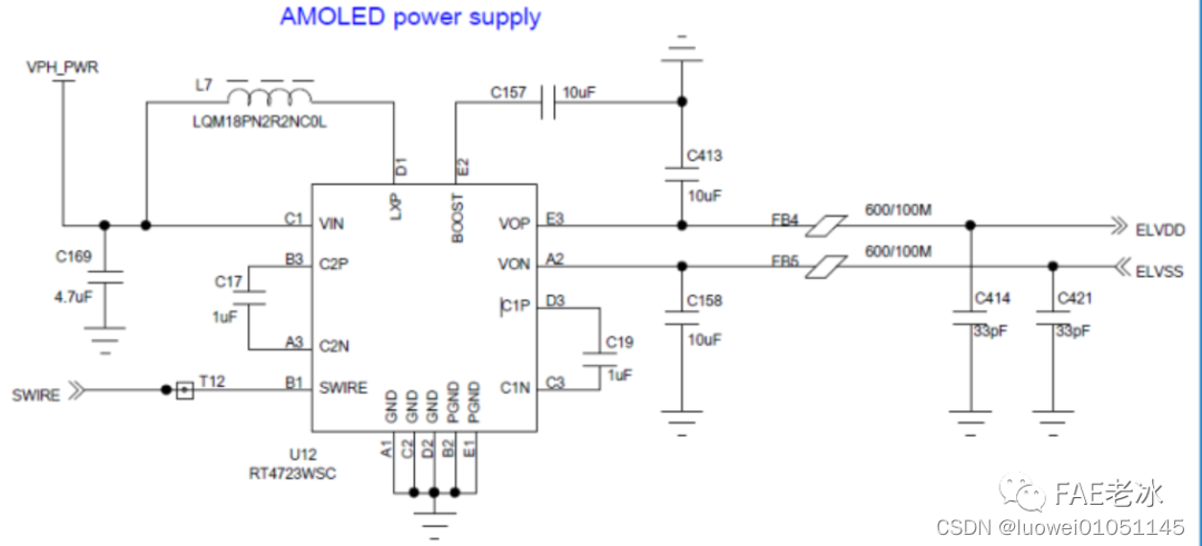
4.1.4 Wireless Bluetooth 、WIFI chip
WCN3620 Three different wireless connection technologies are integrated , Become a device suitable for mobile phones and other mobile devices :
   ⑴  accord with  IEEE 802.11 b/g/n  Standard wireless LAN ( WLAN )

   ⑵  Bluetooth compliant  4.0  Specification version (BR/EDR+BLE) Bluetooth function
WCN3620 It is a highly integrated integrated circuit , Handled by modem IC , To create a wireless connectivity solution , Reduce the number of components and PCB area . The chip adopts low power consumption 65nm radio frequency CMOS Manufacturing technology , It is suitable for battery operated equipment that requires power consumption and performance .
In Bluetooth WIFI GPS Three in one antenna , because GPS Signal processing is not done by WCN3620 Handle , So received GPS After the signal is filtered and amplified by the duplexer , Enter the RF transceiver WTR2965.
BGU8103 It is an ultra-low current and low noise GPS signal amplifier .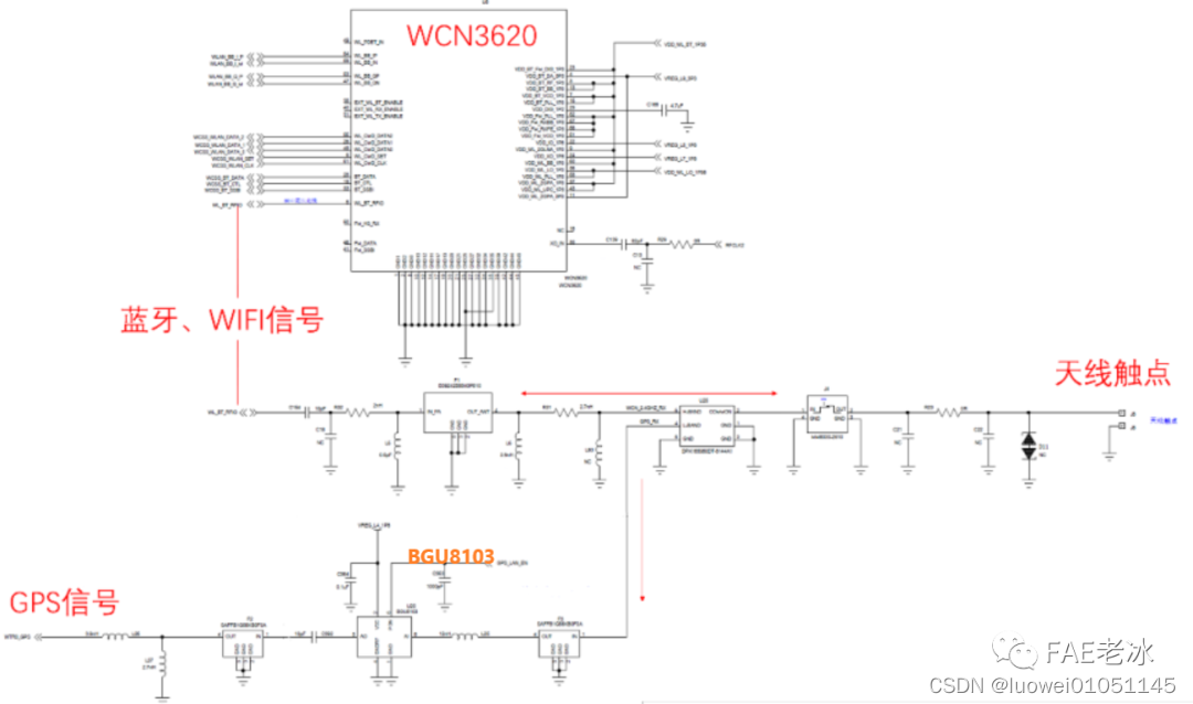
external LDO Power supply chip MM3464 Is a low power consumption 、 High ripple rejection ratio 、 High response voltage regulator , for WCN3620 Provide stable power supply .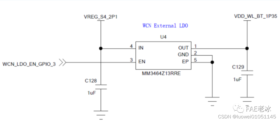
4.1.5 Six axis sensors
LSM6DSLTR It's an accelerometer and gyroscope , Can be found in 0.65mA Working in high-performance mode , And always support low power consumption , Provide consumers with the best sports experience .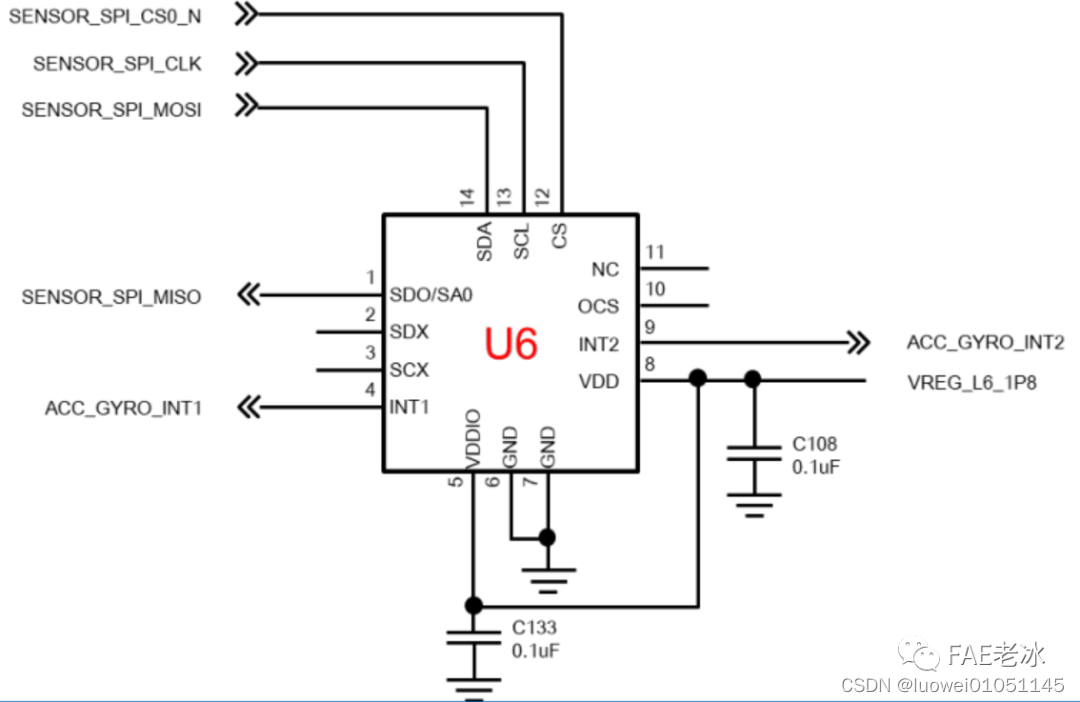
4.1.6 Rf module
The watch communication module is mainly composed of RF transceiver / Power amplifier module / Filter circuit / Front end module / Antenna composition .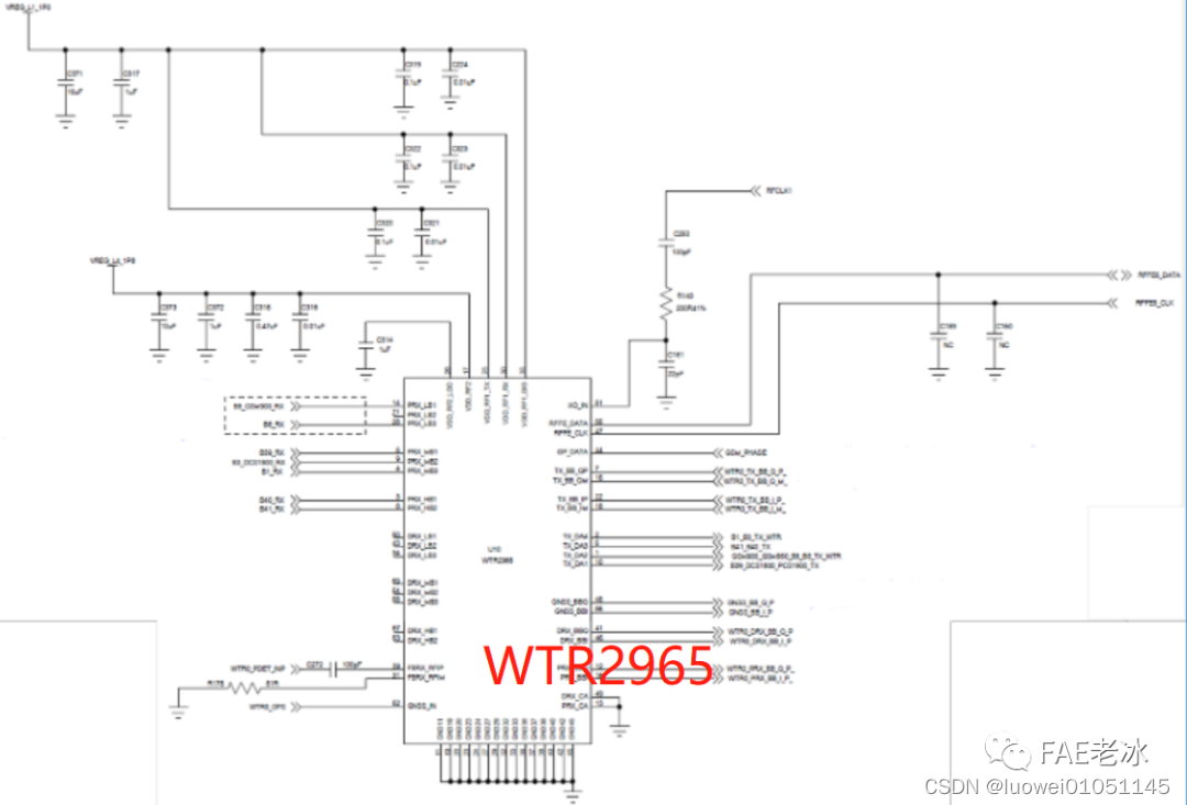
WTR2965 It's a RF transceiver , It is used to process the reception and transmission of RF signals .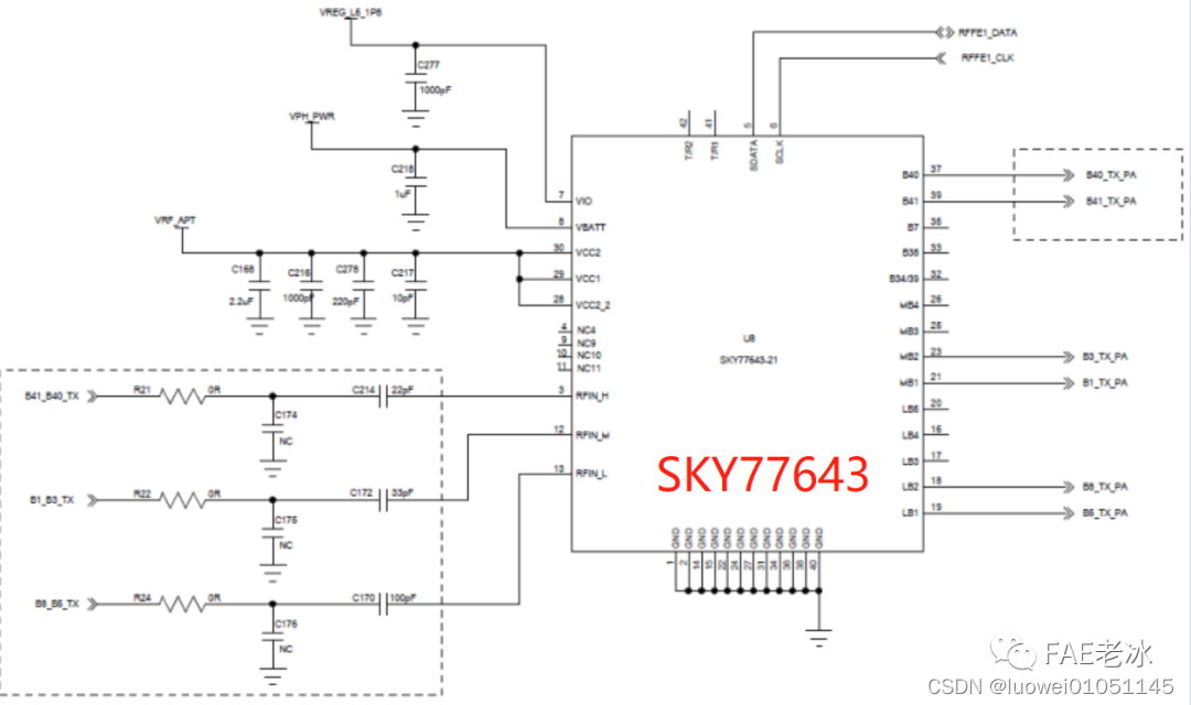
SKY77643 It is the key module to realize the five mode front-end . As a hybrid multi-mode multi frequency power amplifier module ,SKY 77643 Support 3G/4G The Internet , Can be found in WCDMA、TD-SCDMA and LTE Run efficiently in mode . This module includes for low frequency 、 High frequency and intermediate frequency WCDMA/LTE modular , A multifunctional control ( MFC) Block and RF Input / Output port ; Highly integrated features minimize external components .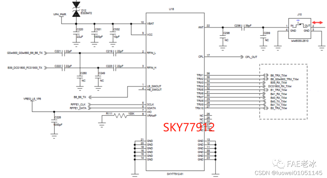
SKY77912 It is a transceiver front-end module ( tx / rx FEM ), Provide complete transmission - Antenna and antenna - receive saw Filter solutions , That is, multiple filter circuits are connected externally .VPH_PWR For input power ,VREG_L5_1P8 by LDO Power input ,SKY77912 Of 22 The foot is connected to the antenna .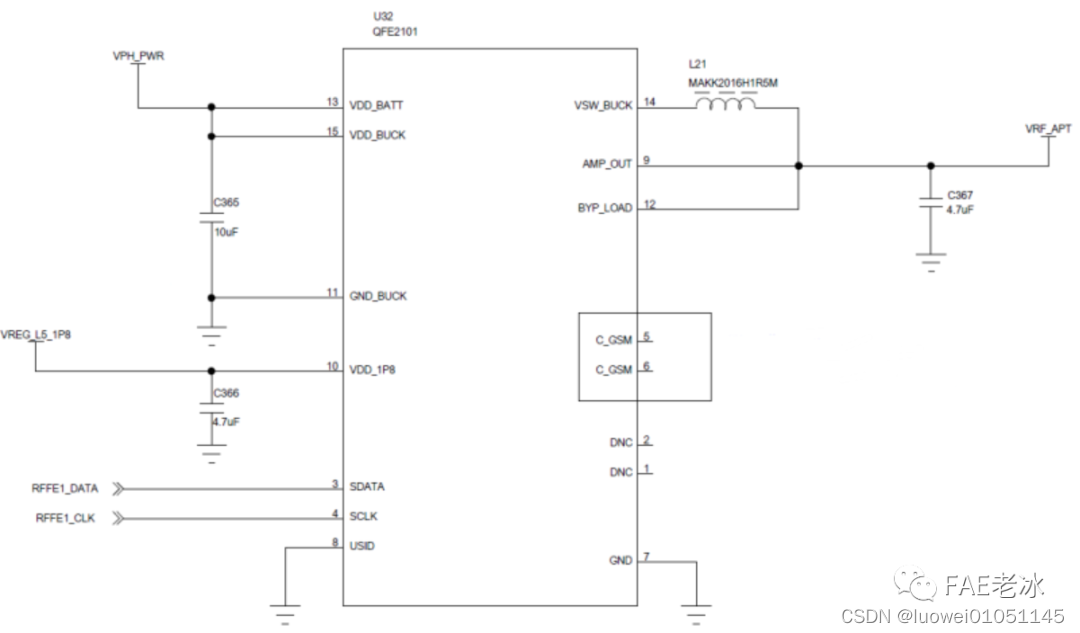
QFE2101 It is a power management IC , It realizes power tracking technology as part of the overall RF front-end solution , Support APT technology , Realize the optimal control of battery power and efficiency .VPH_PWR For power , from IC Of 13 and 15 Foot input ;VREG_L5_1P8 by LDO Power Supply ;RFFE1_DATA For data signal pin ,RFFE1_CLK For clock signal pin ;VRF_APT For output power , Input to SKY77643 Amplification module .
4.1.7 SIM cassette 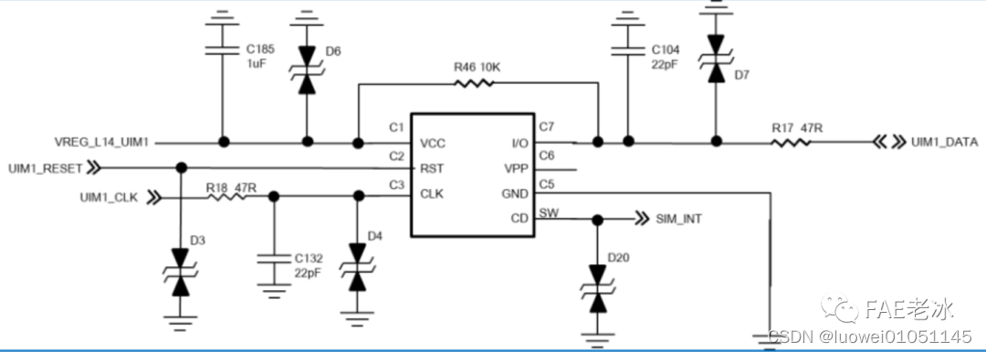
SIM Card seat and previous Y It's one more than a watch SIM_INT function , It is mainly used for hot plug function , Unplug the phone card without turning off the machine .VCC It's the power pin ,RST It is the reset signal pin ,CLK It's the clock signal pin ,I/O It is the data signal pin ,VPP It is a pin for programming ,GND Grounding ,CD It is used for SIM_INT Function pin .
4.1.8 USB Interface 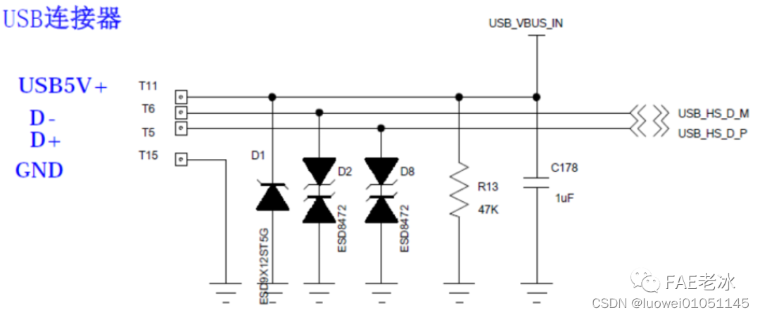
It is used to connect the data line charging and burning system .USB 5V+ Input power supply voltage for external ,D- and D+ by USB Data pins ,GND Grounding .D1 Prevent the instantaneous input voltage from being too high , Avoid machine damage due to high voltage ;D2 and D8 Prevent static electricity from damaging the data transmission function .
2.2.9 Microphone 、 Horn and motor connection circuit 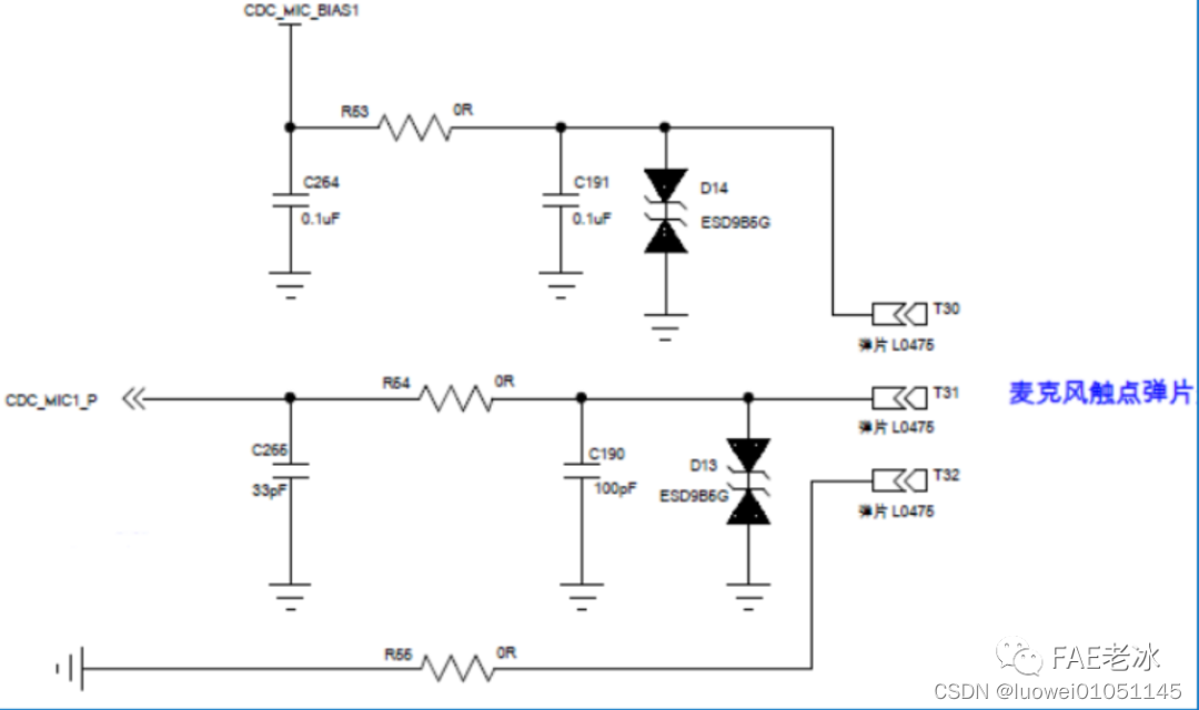
CDC_MIC_BIAS1 The pin provides a bias voltage ,CDC_MIC1_P Receive sound signals .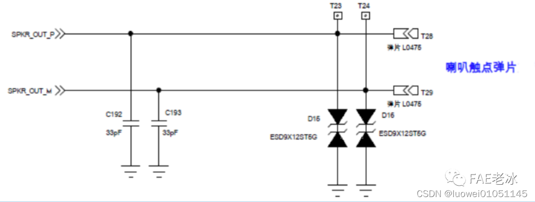
SPKR_OUT_P and SPKR_OUT_P Pin connection horn , Output sound signal .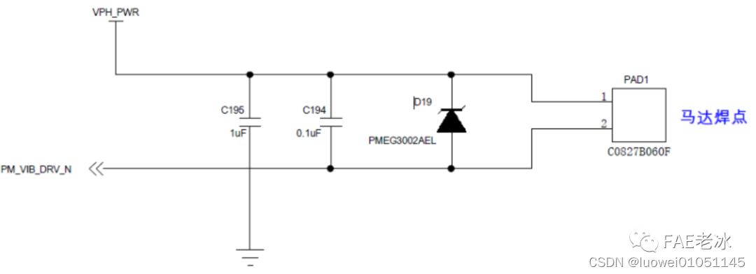
VPH_PWR Provide motor power ,PM_VIB_DRV_N The pin controls the operation of the motor .
4.1.9 Charging current 

This article is reprinted from personal official account , Welcome to exchange , Welcome to follow individual public number “FAE Old ice ”
边栏推荐
- Pytoch temperature prediction
- List and set
- Raspberry pie tap switch button to use
- MongoDB
- JS object and event learning notes
- Analysis of charging architecture of glory magic 3pro
- arduino获取数组的长度
- 共用体(union)详解【C语言】
- Feature of sklearn_ extraction. text. CountVectorizer / TfidVectorizer
- Several declarations about pointers [C language]
猜你喜欢

Programmers can make mistakes. Basic pointers and arrays of C language
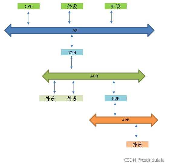
AMBA、AHB、APB、AXI的理解
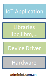
IOT system framework learning
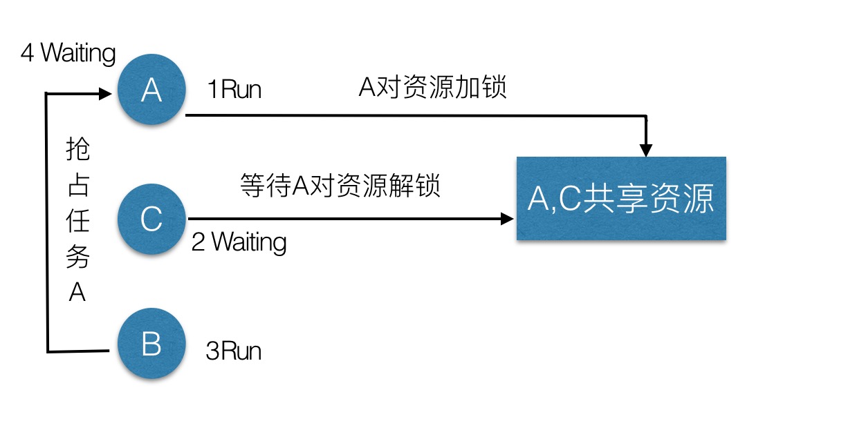
Priority inversion and deadlock
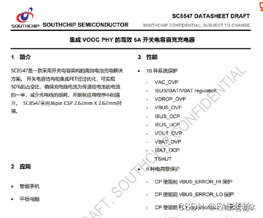
Reno7 60W super flash charging architecture

Linux yum安装MySQL
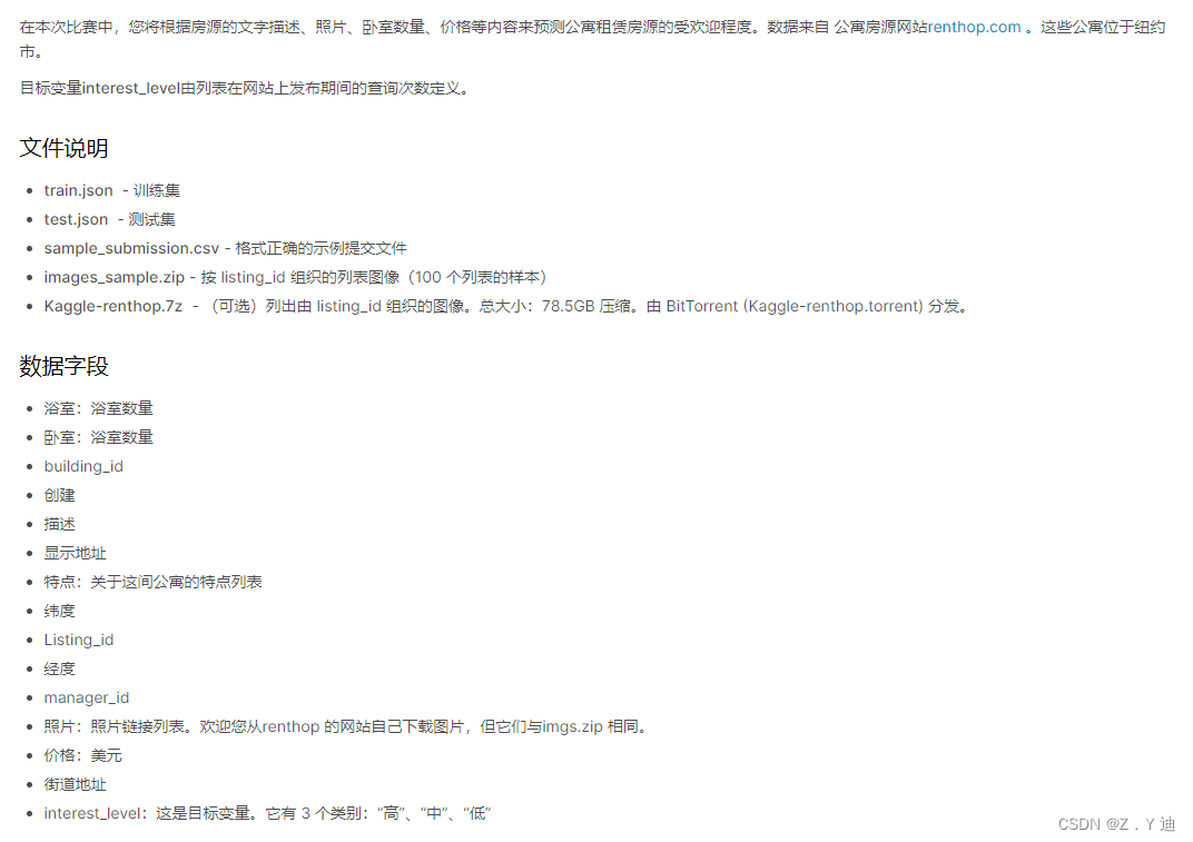
Kaggle竞赛-Two Sigma Connect: Rental Listing Inquiries
![[esp32 learning-2] esp32 address mapping](/img/ee/c4aa0f7aed7543bb6807d7fd852c88.png)
[esp32 learning-2] esp32 address mapping
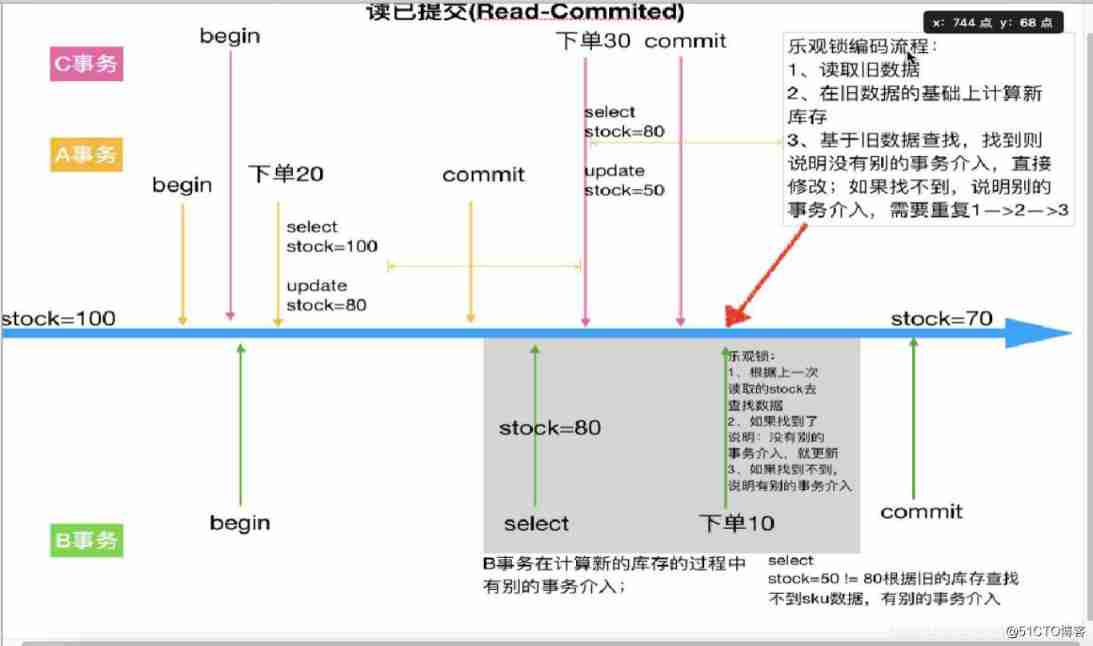
Mall project -- day09 -- order module
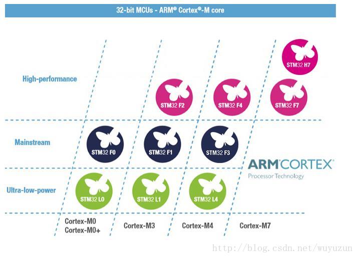
STM32型号与Contex m对应关系
随机推荐
XML文件详解:XML是什么、XML配置文件、XML数据文件、XML文件解析教程
【ESP32学习-2】esp32地址映射
物联网系统框架学习
C语言,log打印文件名、函数名、行号、日期时间
Arm pc=pc+8 is the most understandable explanation
Basic knowledge of lithium battery
There are three iPhone se 2022 models in the Eurasian Economic Commission database
Hutool中那些常用的工具类和方法
Machine learning -- linear regression (sklearn)
PyTorch四种常用优化器测试
map文件粗略分析
Pytoch temperature prediction
Gallery之图片浏览、组件学习
open-mmlab labelImg mmdetection
B tree and b+ tree of MySQL index implementation
Embedded startup process
MySQL数据库面试题
vim命令行笔记
关键字 inline (内联函数)用法解析【C语言】
ESP学习问题记录