当前位置:网站首页>Charge pump boost principle - this article will give you a simple understanding
Charge pump boost principle - this article will give you a simple understanding
2022-07-05 08:09:00 【Learning notes of hardware Xiaobai】
Charge pump , A noun that sounds very tall , Its circuit design is actually applied to many fields . It can not only achieve the purpose of boosting , It can also be used to generate negative pressure . According to its principle , Let's understand it by ourselves , There is no need for Xiaobian to copy and paste online articles !
Take the field in which Xiaobian is engaged , It is mainly integrated in the charging chip .
Design of charge pump circuit , It's not hard to say , Because if you want to design , It can be designed simply . Let's make it simple , It can't be simple , Because Xiaobian has seen the use of very complex charge pumps , But anyway , The truth is the same after all .
So , Based on the situation encountered at work , Today, I still want to talk about the circuit design that uses the charge pump to boost the voltage .
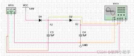
The diagram shows the design of the simplest boost circuit .
XFG1 The peak value provided is 5V The frequency is 10KHz The square wave . So the circuit can be from XFG1 High and low levels are analyzed .
Without considering the diode voltage drop
(a) When XFG1 Input is 0V when , here VCC adopt D1 And D2 by C3 C4 Charge , here A2 B2 The point voltage is 5V.
(b) When XFG1 Input is 5V when , It can be equivalent to two 5V The power supply is connected in series , here A2 The instantaneous voltage at point is 10V, because A2 And B2 There is a differential pressure , So the charge will change from A2 flow B2, As time goes by , Final C3 Voltage and C4 The average is equal , Are all 7.5V. here C3 The pressure difference between positive and negative electrodes is 2.5V.
When XFG1 Input again 0V when , Since the capacitance voltage cannot be changed suddenly , So at this time A2 The point voltage is 2.5V. because D2 The existence of C4 The charge of cannot flow to C3,VCC Charge flow C3,C3 It will soon be charged to 5V.
(4) When XFG1 Input is 5V when ,C3 The state of is back (b) The state of , The upper voltage is 10V, The charge continues to flow C4, Final A2 B2 Both voltages are 8.75V.
(5)XFG1 Such repeated high-low level conversion .C3 The voltage of is also XFG1 For the high time , The instantaneous voltage at the upper end becomes 10V, It keeps giving C4 Charge , therefore C4 The upper voltage keeps rising , To the end C4 The upper voltage is 10V when , No longer transfer charge , At this time, the output voltage is 10V, by VCC Double of , It plays the role of boosting .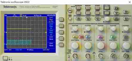
Due to the existence of diode, about 0.4V Pressure drop of , So the final output voltage is a little different from the ideal value .
Such a simple charge pump boost circuit is designed , The principle is also roughly the same . Understand the circuit design , We can also extend by ourselves , Design triple boost , Quadruple boost, etc , This depends on everyone to play !
边栏推荐
- Anonymous structure in C language
- Gradle复合构建
- My-basic application 1: introduction to my-basic parser
- Network communication model -- Network OSI tcp/ip layering
- Volatile of C language
- Soem EtherCAT source code analysis attachment 1 (establishment of communication operation environment)
- Record the visual shock of the Winter Olympics and the introduction of the screen 2
- VESC Benjamin test motor parameters
- Shape template matching based on Halcon learning [VII] reuse_ model. Hdev routine
- 动力电池UL2580测试项目包括哪些
猜你喜欢
![C WinForm [display real-time time in the status bar] - practical exercise 1](/img/9f/d193cbb488542cc4c439efd79c4963.jpg)
C WinForm [display real-time time in the status bar] - practical exercise 1
Classic application of MOS transistor circuit design (1) -iic bidirectional level shift

研究发现,跨境电商客服系统都有这五点功能!
Improve lighting C program
Semiconductor devices (I) PN junction
Talk about the circuit use of TVs tube
![[tutorial 19 of trio basic from introduction to proficiency] detailed introduction of trio as a slave station connecting to the third-party bus (anybus PROFIBUS DP...)](/img/54/2fe86f54af01f10de93818103f2154.jpg)
[tutorial 19 of trio basic from introduction to proficiency] detailed introduction of trio as a slave station connecting to the third-party bus (anybus PROFIBUS DP...)
DokuWiki deployment notes
![Halcon's practice based on shape template matching [1]](/img/68/206eed7502fbf108a929aa9365b1ae.jpg)
Halcon's practice based on shape template matching [1]

UEFI development learning 5 - simple use of protocol
随机推荐
Management and use of DokuWiki (supplementary)
Altium designer learning (I)
List of linked lists
IEEE access personal contribution experience record
Tailq of linked list
Detailed explanation of SQL server stored procedures
Factors affecting the quality of slip rings in production
Nb-iot technical summary
matlab timeserise
L'étude a révélé que le système de service à la clientèle du commerce électronique transfrontalier a ces cinq fonctions!
Live555 push RTSP audio and video stream summary (III) flower screen problem caused by pushing H264 real-time stream
找不到实时聊天软件?给你推荐电商企业都在用的!
C WinForm [view status bar -- statusstrip] - Practice 2
[trio basic tutorial 18 from introduction to proficiency] trio motion controller UDP fast exchange data communication
Shape template matching based on Halcon learning [9] PM_ multiple_ dxf_ models. Hdev routine -- [read and write XLD from DXF file]
2021-10-28
Train your dataset with yolov4
1-stm32 operation environment construction
UEFI development learning 6 - creation of protocol
[tutorial 15 of trio basic from introduction to proficiency] trio free serial communication