当前位置:网站首页>Ethernet port &arm & MOS &push-pull open drain &up and down &high and low sides &time domain and frequency domain Fourier
Ethernet port &arm & MOS &push-pull open drain &up and down &high and low sides &time domain and frequency domain Fourier
2022-07-06 03:38:00 【woshizuopie】
Catalog
2.3 What is an instruction set :
3.4 Power chip selection LDO still DC-DC?
4. Push pull output and open drain output
7. Time domain 、 frequency domain 、 Fourier analysis
Excel How to multiply a column of a table by the same number
excel How to apply the formula to the whole column
1. Ethernet
Reference resources :
Internet Literacy 1 : Preliminary understanding of network card
Internet Literacy II :Mac And Phy A simple analysis of the principle of composition
Internet Literacy III : Ethernet chip MAC and PHY The relationship between
Introduction to Internet port
Network adapter is also called network card (NIC:Network Interface Card), It's a device that connects computers to the Internet .
working principle : The computer writes the data to be transmitted to the cache of the network card in parallel , The network card encodes the data to be transmitted , Serially sent to the transmission medium . The opposite is true when receiving data .
Usually, the network card uses 20 or 25MHz The crystal oscillator , Gigabit network card use 62.5 or 125MHz The crystal of .
The network port is controlled by CPU、MAC and PHY Three parts .DMA The controller usually belongs to CPU Part of , Put the dotted line here to indicate DMA The controller may participate in the data transmission of network interface .
For the above three parts , There are several types of combinations :
1. CPU Integrate MAC And PHY;
2. CPU Integrate MAC,PHY Using independent chip ;
3. CPU No integration MAC And PHY,MAC And PHY Adopt integrated chip .
Next, select two pairs of schemes MAC And PHY Between MII Explain the interface .
Here's the picture , Phantom representation CPU,PHY The chip passes through MII Interface and CPU Upper MAC Connect .
In software, the operation of the network interface is usually divided into the following steps :
1.  Allocate memory for data sending and receiving ;
2.  initialization MAC register ;
3.  initialization PHY register ( adopt MIIM);
4.  Start sending and receiving .
MII
MII Media independent interface , Including a data interface , And one. MAC and PHY Management interface between . The data to be sent is sent through MII The transceiver in the interface is realized by two groups of buses , And yes PHY Configuration information of chip register , Through MII A group of serial port bus implementation , namely MIIM(MII Management).
MIIM There are only two lines : Clock signal line MDC And data lines MDIO. The read and write commands are controlled by MAC launch ,PHY Cannot pass MIIM Active direction MAC Send a message . So we can only operate MAC Register on .
DMA
Sending and receiving data makes DMA To do it ,CPU Just tell me DMA Just start length and address .
Usually MAC There will be a set of registers in the to record the data address (tbase and rbase),CPU Press MAC Put the data in the correct format , start-up MAC Just send the data . Registers are usually used during startup tstate.
MAC
MAC(Media Access Control, Media access control sublayer protocol ).
CPU There are two sets of registers on MAC. One group is used for data sending and receiving , Corresponding to the above DMA; One set for MIIM, Used to deal with PHY To configure . Both sets of registers are in CPU On , The configuration method is the same as other methods CPU Same as the upper register , Just read and write directly .
PHY

PHY The chip has a set of registers for storing the configuration , And update the status .CPU This set of registers cannot be accessed directly , Only through MAC Upper MIIM Register groups achieve indirect access . meanwhile PHY The chip is responsible for MII Bus data and Media Interface Data forwarding on .
2. Arm
2.1 What is? ARM kernel :
So called kernel , Namely CPU It is the core of computing , We can also call the kernel CPU.ARM Kernel is just a general term , It has the following series :ARM7,ARM9,ARM11,Cortex Wait for several kernel families , Each kernel family has different kernel types . such as CORTEX The kernel family has :Cortex-A9 kernel 、Cortex-R4 kernel 、Cortex-M3 Kernel, etc , At present, the most widely used STM32 Series chips use Cortex-M3 kernel .
2.2 What is? ARM framework :
On one side , We can understand the architecture as the instruction set used by the kernel .ARM The architecture of is based on RISC Instruction set based , And its kernel is only the basis of the hardware architecture to realize this instruction set .
for example : For high-end ( Mobile phone etc. )Cortex-A8,Cortex-A9 Wait for the kernel to use ARMv7-A framework , Or use ARMv7-A Instruction set architecture , We often use it STM32 Of Cortex-M3 The kernel uses ARMv7-M framework .
2.3 What is an instruction set :
The so-called instruction set is the general name of a set of low-level instructions . It is divided into RISC( Simple instruction set ) and CISC( Complex instruction set ), By comparison RISC The instruction format of instruction set is unified , There are fewer species , There are fewer addressing modes than complex instruction sets , and CISC The efficiency of instruction set is relatively high .
take STM32 Series chips used ARMv7 Instruction set ,ARMv7 intend ARM The seventh version of the directive , Adopted RISC.
3. mos Field effect tube
3.1 NMOS and PMOS

There is another way to express :( This symbol can also represent NMOS and PMOS, But this kind is usually used in the internal circuit of the chip , The external circuit still uses the above two symbols ).
The following figure shows the knowledge in the learning video :
We often use devices working in the switching state to form digital circuits or logic gates .
as follows , Namely N transistor 、N Type FET 、P Type FET . When high voltage is applied ,N Collector and emitter of type a transistor ( Or is it N The source and drain of type a FET ) Is the conduction state .
The transistor is abstracted as a switch , They are 1 Conduction 、 Or by the 0 Conduction .
also eg:
Here's the picture : The upper and lower switches are complementary . So here it is A high voltage ,B It will output low voltage , Because the bottom is conductive ; to A Low voltage ,B It will output high voltage , Because the top is conductive .
3.2 Vcc、Vdd、Vss
Vcc: The supply voltage of the circuit .
Vdd: Working voltage inside the chip .
Vss:s=series Indicates a public connection , It usually refers to the voltage at the common ground terminal of the circuit .
Vpp: Programming / Erase voltage .
(1) For digital circuits , Usually Vcc>Vdd,Vss It's the ground point .
(2) There are some IC both Vdd The pin has Vcc Pin , It shows that the device has voltage conversion function .
(3) Electrically ,GND It is divided into power supply and ground (PG) And signally (SG). The other two kinds of places that are distinguished by different circuit forms are : Digitally 、 Simulate . In general ,Vcc= Analog power ,Vdd= Digital power supply ,Vss= Digitally ,Vee= Negative power supply .
(4)Vcc From collector voltage ,Collector Voltage, Generally used for bipolar transistors ;
Vdd From drain supply voltage ,Drain Voltage, stay MOS In transistor circuit , Generally connected to MOS The drain pin of the tube , Correct the power supply ;
Vss From the source supply voltage , stay MOS The transistor circuit is connected to the source , Refers to negative power supply .
3.3 LDO
One model is “TPS7B6350-Q1” Chip ,datasheet There is a “300mA 40V High-Voltage Ultralow Quiescent-Current Watchdog LDO”, So let's know what is LDO?
LDO: Low differential linear voltage regulator (low dropout regulator),
This is relative to the traditional linear regulator . Traditional linear regulators may require that the input voltage of the chip be at least higher than the output voltage 2-3V, Otherwise it won't work properly . But in some cases , for instance 5V turn 3.3V No way. , So I invented LDO.
LDO The main circuit diagram of is as follows : Its core lies in the transistor in the circle ( You can make MOSFET or BJT), It uses transistors to work in the linear region , The channel resistance can be controlled by controlling the grid voltage to control the output voltage . But it can only reduce blood pressure , If you want to boost voltage, you should choose DC-DC perhaps charge pump.
But how to realize automatic adjustment Vout? As shown in the figure ,R1、R2 The sampling voltage composed of is connected to the in-phase terminal of the error amplifier , Then connect a reference voltage to the reverse end of the error amplifier ( The polarity cannot be reversed, otherwise it cannot be amplified ), as long as Vout If there is a change, the sampling voltage is the same as Vref The voltage difference will be amplified and output to gate So as to adjust the input and output characteristics of the transistor , Achieve adjustment Vout The effect of . This is a dynamic correction process , So it's called a voltage regulator .
3.4 Power chip selection LDO still DC-DC?
LDO It is equivalent to a resistive partial voltage to realize voltage reduction ,DC-DC The energy loss is not obvious in the process of pressure reduction , The chip package is small , It can be realized PWM Digital control . in general , Boost pressure must be selected DCDC Of , step-down , It's choice DCDC still LDO, At the cost of , efficiency , Noise and performance comparison .
choose LDO when : The output current is not large (3A within ), The input and output voltage difference is not big . When considering sensitive analog circuits , You have to sacrifice DC-DC High efficiency and choose low noise LDO.
3.5 TTL、CMOS
(1) TTL High level 3.6-5V, Low level 0-2.4V;CMOS level Vcc Accessible 12V,CMOS The circuit output high level is about 0.9Vcc, The output low level is about 0.1Vcc.
(2) TTL The level is 5V,CMOS The level is generally 12V, because TTL The circuit supply voltage is 5V,CMOS The circuit power supply voltage is generally 12V.
(3) TTL Level standard :
Output L:<0.8V;H:>2.4V.
Input L:<1.2V;H:>2.0V.
namely ,TTL The output low level of the device should be less than 0.8V, The high level is greater than 2.4V. Input , lower than 1.2V Think of it as 0, higher than 2.0 Think of it as 1.
CMOS level :
Output L:<0.1Vcc;H:>0.9Vcc.
Input L:<0.3Vcc;H:>0.7Vcc.
4. Push pull output and open drain output
In the above code ,IfxPort_setPinModeOutput Set the pin to push-pull output .
Reference resources What is push-pull output ?.
First of all, understand the principle of triode .NPN The basic structure of type a triode is as follows : The base (Base)、 Collector (Collector) And the emitter (Emitter).
This triode is a current controlled component , As long as B Extremely input ( Or output ) Current can control this transistor .
Change the concept , Base B Regarded as the control end 、 Collector C As input , The emitter E Regarded as output , Input and output refers to the direction of current flow . When there is current input at the control terminal , Current will enter from the input and flow out from the output . as follows :
PNP Tube is just the opposite :
So push-pull circuit :
Notice that it's N type , Here is P type .
When Vin Voltage is V+ when , above N The control terminal of type a triode has a current input ,Q3 Conduction , So the current goes from top to bottom , Supply current to the load . This is called pushing .
When Vin Voltage is V- when , There is current flowing out of the lower triode ,Q4 Conduction ,Q4 There is current flowing from top to bottom . Go through the following P Type triode provides current to the load , This is called Wan .
above , Namely push-pull circuit ***(push-pull).
So what is open leak ?
To understand first The opening episode *. It's the collector C Nothing at one end , Directly as an output port .
If you want to carry a load for this circuit , For example, a LED, A pull-up resistor must be connected , as follows :
When Vin No current ,Q5 When disconnected ,LED bright ; When Vin Incoming current ,Q5 Conduction time ,LED destroy .
Open drain circuit Is to replace the triode in the figure above with a field effect transistor (MOSFET).N Type FET is as follows :
FET is a voltage controlled component , Just apply voltage to the grid ,DS It's going to turn on .
The difference between Junction FET and triode :
The input impedance of Junction FET is very large , This means that no current is input from the control circuit , There is no current output , It won't burn out the control circuit . And triode is a current controlled component , If an open set circuit is used , It may burn out the circuit . therefore Open drain circuits have replaced open set circuits .
5. Pull up 、 The drop-down

6. high 、 Low side drive
There are two ways to drive loads : Low side drive 、 High side drive . The low side drive is usually used for loads related to the powertrain , For example, the motor 、 Heater ; High side drive is often used for fuel pump and body related functions , Such as seats 、 lighting 、 Wiper 、 Fans, etc .

7. Time domain 、 frequency domain 、 Fourier analysis
Signal analysis , Why do we often use some transformations to transform the signal into frequency domain for analysis ?
answer : Because some operations are easier to implement in the frequency domain , Like convolution , Convolution is signal filtering 、 The basis of correlation operation . Especially when FFT When it appears , By transforming the time domain signal to the frequency domain, the amount of computation can be greatly reduced . Some signals are more intuitive in the frequency domain , Combining amplitude frequency and phase frequency characteristics . Time domain and frequency domain are two methods to characterize signals , The two are equivalent in reflecting signal characteristics , It's just a different angle .
Explain Fourier transform in simple terms
Methods throughout time domain and frequency domain —— Fourier analysis
8. Excel skill
Excel How to multiply a column of a table by the same number
Excel How to multiply a column of a table by the same number
excel How to apply the formula to the whole column
边栏推荐
- BUAA计算器(表达式计算-表达式树实现)
- Distributed service framework dobbo
- 3.1 rtthread 串口设备(V1)详解
- Tidb ecological tools (backup, migration, import / export) collation
- Remote Sensing Image Super-resolution and Object Detection: Benchmark and State of the Art
- BUAA喜鹊筑巢
- [prediction model] difference method model
- Mysqldump data backup
- Indicator system of KQI and KPI
- Data analysis Seaborn visualization (for personal use)
猜你喜欢
Data analysis Seaborn visualization (for personal use)
Svg drag point crop image JS effect
Multi project programming minimalist use case

pytorch加载数据
Precautions for single chip microcomputer anti reverse connection circuit

指针笔试题~走近大厂
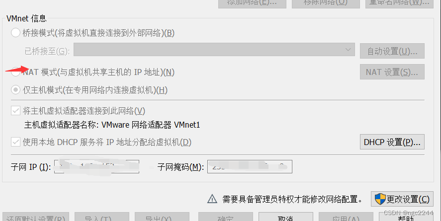
The real machine cannot access the shooting range of the virtual machine, and the real machine cannot Ping the virtual machine
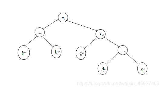
BUAA calculator (expression calculation - expression tree implementation)

three. JS page background animation liquid JS special effect

The ECU of 21 Audi q5l 45tfsi brushes is upgraded to master special adjustment, and the horsepower is safely and stably increased to 305 horsepower
随机推荐
Remote Sensing Image Super-resolution and Object Detection: Benchmark and State of the Art
[risc-v] external interrupt
Microsoft Research, UIUC & Google research | antagonistic training actor critic based on offline training reinforcement learning
MADDPG的pythorch实现——(1)OpenAI MADDPG环境配置
Cubemx transplantation punctual atom LCD display routine
Pytoch foundation - (1) initialization of tensors
Lua uses require to load the shared library successfully, but the return is Boolean (always true)
下一个行业风口:NFT 数字藏品,是机遇还是泡沫?
Codeforces Global Round 19
svg拖动点裁剪图片js特效
真机无法访问虚拟机的靶场,真机无法ping通虚拟机
Pointer written test questions ~ approaching Dachang
2.2 STM32 GPIO操作
mysql从一个连续时间段的表中读取缺少数据
SWC introduction
【Rust 笔记】18-宏
2.1 rtthread pin device details
Tidb ecological tools (backup, migration, import / export) collation
关于非虚函数的假派生
The next industry outlet: NFT digital collection, is it an opportunity or a foam?