当前位置:网站首页>SPI communication protocol
SPI communication protocol
2022-07-06 01:55:00 【Clear glass, brilliant orange】
SPI(Serial Peripheral Interface, Serial peripheral interface ) Motorola (Motorola) stay 1980 A kind of all double Synchronous serial communication interface , It is used for MCU Communicate with various peripheral devices in serial mode to exchange information , The communication speed can reach up to 25MHz above .
SPI The interface is mainly used in EEPROM、FLASH、 Real time clock 、 Network controller 、OLED Display drive 、AD converter , Digital signal processor 、 Between digital signal decoder and other equipment .
SPI It usually consists of four lines , A master output and a slave input (Master Output Slave Input,MOSI), One main equipment Standby input and slave output (Master Input Slave Output,MISO), A clock signal (Serial Clock,SCLK), One from Device enable selection (Chip Select,CS). And I²C similar , The agreements are simple , You can also use GPIO simulation SPI sequential .
SPI It can send and receive data at the same time , therefore SPI Theoretical transmission speed ratio I²C faster .
however SPI Select the slave through the chip selection pin , Choose one slave for each movie , Therefore, in the multi slave structure , Need to occupy more pins , and I²C Through the equipment Address selection slave , As long as the device address does not conflict , Always only two pins are needed .
SPI One master can connect one or more slaves , Each slave uses a pin for chip selection , The physical connection diagram is shown in Figure 
SPI Schematic diagram of one master and one slave
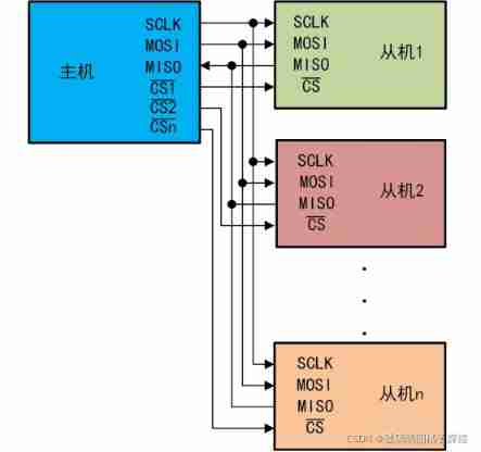
SPI Schematic diagram of one master and many slaves
2**. Data exchange **
stay SCK Driven by the clock cycle ,MOSI and MISO At the same time , As shown in the figure , It can be regarded as a virtual ring topology .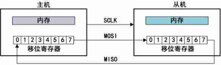
Virtual ring topology
Both master and slave have a shift register, which is also a serial shift register , The host shift register data passes through MOSI Write data to the shift register of the slave , At this time, the data of the serial shift register of the slave also passes MISO To the host , The data exchange between two shift registers is realized . Whether master or slave , Both sending and receiving are done at the same time , Like a “ Ring ”.
If the master only writes to the slave , The host only needs to ignore the received slave data . If the master wants to read the slave data , The master needs to send an empty data to trigger the slave to send data .
STM32F103 Series of SPI controller , It can be used as communication master or slave , Support four complete transmission modes , Support 8 Bit or 16 Bit data length . Every SPI Each controller has a chip select pin NSS, When using this pin as chip selection , It is called hardware chip selection mode , You can also use any It means GPIO As a chip selection pin , It is called software chip selection mode .
SPI The controller structure is shown in the figure , It can be seen as four parts .
① Pin :SPI The protocol requires four pins :MOSI、MISO、SCK、NSS. among NSS You can use any GPIO Instead of , Realize manual chip selection through software control level .
② Data transmission :SPI The transmission of can be regarded as a ring topology . When sending data , Data on the bus is written to the transmit buffer , from Send buffer into shift register , Finally from the MOSI Output . meanwhile ,MISO The data of also enters the shift register , Incoming receive buffer ,
Finally, the bus .
③ Clock signal :SPI Your clock comes from PCLK, By configuring SPI_CR1 The register of BR[2:0] Realize to PCLK Frequency division , Up to fPCLK/2. It can be seen from the previous figure ,SPI1 Mounted on APB2 Upper ,SPI2 It's mounted on APB1 Upper . It can be seen from the previous figure APB2 The highest 72MHz,APB1 The highest 36MHz. therefore SP1 The highest working frequency is fPCLK2/2=36MHz,SPI2 The highest working frequency is fPCLK1/2=18MHz.
④ Main control logic : There are two control registers (Control Register 1,CR1) and (Control Register 2,CR2) For control logic . Through them, you can modify SPI Working mode of (CPOL、CPHA), Configure peripheral clock frequency ,DMA Enable, etc . At the same time, the state of the control logic will be fed back to (Status Register ,SR) On this status register , hear SPI Working state .
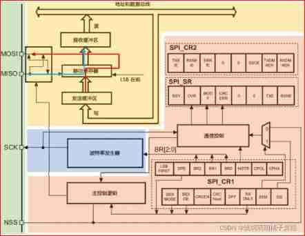
SPI Controller module diagram
3.STM32 Of SPI Interfaces can be configured to support SPI Agreement or support IIS
Audio protocol , The default is SPI agreement , You can also switch to IIS The way .
SPI features
● 3 Line full duplex synchronous transmission
● Two wire simplex synchronous transmission with or without the third bidirectional data line
● 8 or 16 Bit transmission frame format selection
● Master or slave operation
● Support multi master mode
● 8 Baud rate prescaler coefficient of main modes ( The maximum is fPCLK/2)
● From mode frequency ( The maximum is fPCLK/2)
● Fast communication between master mode and slave mode
● Both master mode and slave mode can be controlled by software or hardware NSS management : Lord / From the dynamic change of operation mode
● Programmable clock polarity and phase
● Programmable data sequence ,MSB In front or LSB before
● Dedicated send and receive flags that trigger interrupts
● SPI Bus busy status flag
● Hardware that supports reliable communication CRC
─ In send mode ,CRC The value can be sent as the last byte
─ In full duplex mode, the last byte received is automatically updated CRC check
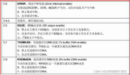
● Main mode failure that triggers interrupts 、 Overload and CRC Error flag , So we can judge the data transmission according to the interrupt flag , Whether to start sending data .
● Support DMA Functional 1 Byte send and receive buffers : Generate send and receive requests
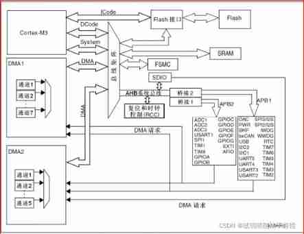
SP1 Connect to APB1 On
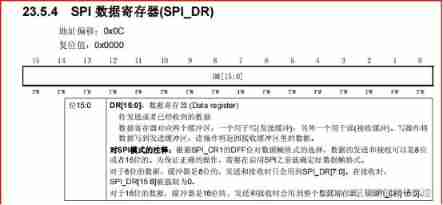
SPI Some registers 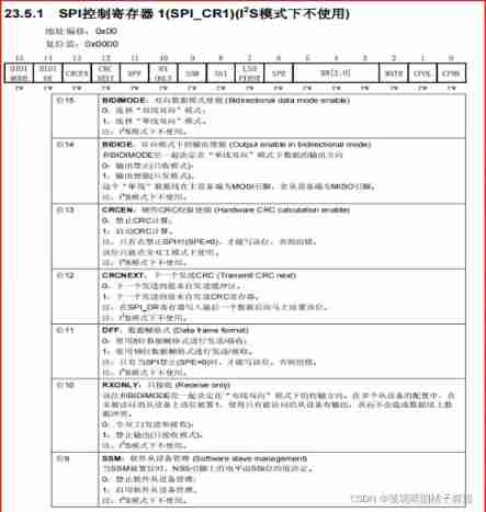
When SSM When set ,NSS The level on the pin is determined by SSI The value of bits determines .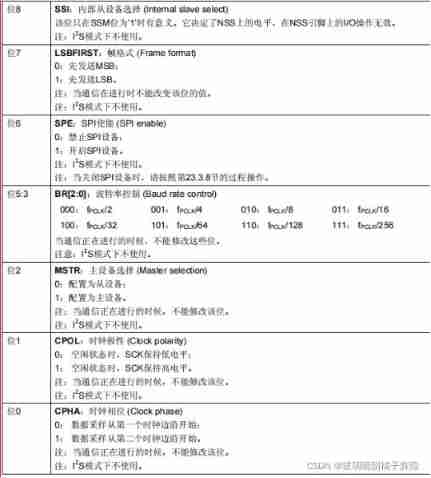
The frame format
0: Send... First MSB; It means to send high bytes first
1: Send... First LSB. It means sending low bytes first
SPE:SPI Can make (SPI enable)
position 6
0: prohibit SPI equipment ;
1: Turn on SPI equipment .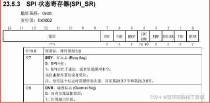
transmission mode
SPI There are four transmission modes , As shown in the table 18.1.2 Shown , The main difference is CPOL and CPHA Different .
CPOL(Clock Polarity, Clock polarity ) Express SCK High level or low level when idle . When CPOL=0,SCK In my spare time, I am
Low level , When CPOL=1,SCK High level when idle .
CPHA(Clock Phase, Clock phase ) Express SCK Sample data at the edge of the clock . When CPHA=0, stay SCK The first side
Sampling data along , When CPHA=1, stay SCK The second edge samples data .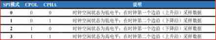
Pictured CPHA=0 when , Indicates that data is sampled at the first clock edge of the clock . When CPOL=1, That is, high level when idle ,
Change from high level to low level , First clock edge ( Falling edge ) I.e. sampling . When CPOL=0, That is, it is low when idle , From low level to high level , First clock edge ( Rising edge ) I.e. sampling .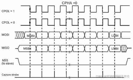
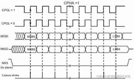
Change from high level to low level and then to high level , Second clock edge ( Rising edge ) I.e. sampling . When CPOL=0, That is, low power when idle
flat , Change from low level to high level and then to low level , Second clock edge ( Falling edge ) I.e. sampling .
SPI Interface mode
1. Data frame format 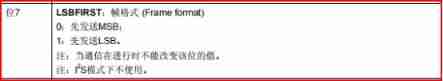
according to SPI_CR1 The register of LSBFIRST position , Output data can be selected MSB( High position ) First or LSB( Low position ) First .
according to SPI_CR1 The register of DFF position , The optional data frame is 8 Bits or 16 position , Valid for both sending and receiving .
2. Status flag
Through three signs, you can fully monitor SPI Status of the bus
Send buffer idle flag (TXE)
This flag is 1 When , Indicates that the transmit buffer register is empty , The next data to be sent can be written into the buffer , When writing SPI_DR( Data register ) when ,TXE The flag is cleared .
The receive buffer is not empty (RXNE)
This flag is 1 Indicates that the receive buffer contains valid data , read SPI The data register can clear this flag .
BSY sign
BSY Signs are set and clear by hardware , This flag indicates SPI Status of communication layer .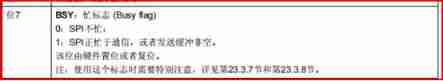
SPI interrupt 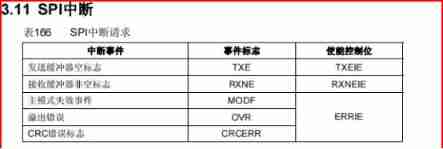
SPI Pin configuration 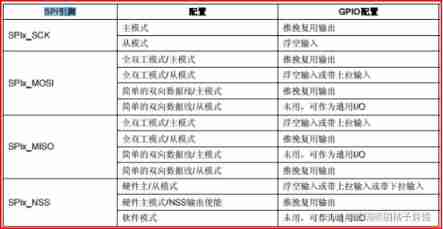
Slave device pin management (NSS)
① Software mode :
You can set SPI_CR1 The register of SSM Bits enable this mode , In this mode NSS Pins can be used for other purposes , And inside NSS The signal level can be determined by writing SPI_CR1 Of SSI Bit to drive .
② Hardware mode :
Case one :NSS Output enable , When STM32 Work for SPI When mode ,NSS The output has passed SPI_CR2 The register of SSOE Bit enable , At this time NSS The pin is pulled low , all NSS Pin with this master SPI Of NSS The pins are connected and configured as hardware NSS Of SPI equipment , Will automatically become slave SPI equipment .
The second case :NSS The output is turned off : Allow operation in multiple master environments .
边栏推荐
- Leetcode skimming questions_ Invert vowels in a string
- Redis守护进程无法停止解决方案
- Leetcode3, implémenter strstr ()
- Folio. Ink is a free, fast and easy-to-use image sharing tool
- ClickOnce 不支持请求执行级别“requireAdministrator”
- NiO related knowledge (II)
- 剑指 Offer 12. 矩阵中的路径
- selenium 元素定位(2)
- 安装Redis
- National intangible cultural heritage inheritor HD Wang's shadow digital collection of "Four Beauties" made an amazing debut!
猜你喜欢
You are using pip version 21.1.1; however, version 22.0.3 is available. You should consider upgradin

XSS learning XSS lab problem solution
Blue Bridge Cup embedded_ STM32_ New project file_ Explain in detail

National intangible cultural heritage inheritor HD Wang's shadow digital collection of "Four Beauties" made an amazing debut!
dried food! Accelerating sparse neural network through hardware and software co design
c#网页打开winform exe

Computer graduation design PHP college student human resources job recruitment network

How to improve the level of pinduoduo store? Dianyingtong came to tell you
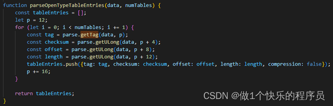
Extracting key information from TrueType font files

Computer graduation design PHP enterprise staff training management system
随机推荐
[understanding of opportunity-39]: Guiguzi - Chapter 5 flying clamp - warning 2: there are six types of praise. Be careful to enjoy praise as fish enjoy bait.
【网络攻防实训习题】
[technology development -28]: overview of information and communication network, new technology forms, high-quality development of information and communication industry
安装Redis
Format code_ What does formatting code mean
GBase 8c数据库升级报错
干货!通过软硬件协同设计加速稀疏神经网络
Code review concerns
Paddle框架:PaddleNLP概述【飞桨自然语言处理开发库】
A Cooperative Approach to Particle Swarm Optimization
TrueType字体文件提取关键信息
Basic operations of database and table ----- set the fields of the table to be automatically added
module ‘tensorflow. contrib. data‘ has no attribute ‘dataset
正则表达式:示例(1)
Computer graduation design PHP college classroom application management system
Mongodb problem set
[network attack and defense training exercises]
internship:项目代码所涉及陌生注解及其作用
Redis-Key的操作
Basic operations of databases and tables ----- unique constraints