当前位置:网站首页>21. [STM32] I don't understand the I2C protocol. Dig deep into the sequence diagram to help you write the underlying driver
21. [STM32] I don't understand the I2C protocol. Dig deep into the sequence diagram to help you write the underlying driver
2022-07-05 15:48:00 【According to point_ DW】
Author's brief introduction : Hello, everyone , My name is DW, Share some of my new knowledge every day , Look forward to making progress with you
Series column :STM32
Development board :STM32F103If there is anything that is not well written, you are welcome to correct
Creation time :2022 year 7 month 3 Japan
I2C(Inter-Integrated Circuit BUS) For integrated circuit bus , The bus is controlled by NXP Company design , It is mainly used for master-slave communication between master controller and slave devices .IIC and SPI Strictly speaking, interfaces are a combination of software and hardware defined by people , It is divided into physical layer and protocol layer .
SDA(Serial data) It's the data line , It is used to transmit data .
SCL(Serial clock line) It's a clock line , It controls the timing of data transmission .

I2C The three most important points are :
1. Start and end conditions
2. Reply and non reply
3. The validity of the data
below , I will introduce how to use these three important knowledge points one by one , Because of the SDA Output and input mode selection , So first configure its output and input modes .
// Mode configuration  out input
void I2C_Mode(u8 addr){

	GPIO_InitTypeDef GPIO_InitStructure;

	if(addr){  //out
		GPIO_InitStructure.GPIO_Pin = SDA;//PB0
		GPIO_InitStructure.GPIO_Speed = GPIO_Speed_50MHz;// Output rate
		GPIO_InitStructure.GPIO_Mode = GPIO_Mode_Out_PP;// Push pull output
	}
	else{  //Input
		GPIO_InitStructure.GPIO_Pin = SCL;//PB1
		GPIO_InitStructure.GPIO_Mode = GPIO_Mode_IPU;// Push pull output
	}
		GPIO_Init(I2C_PROT,&GPIO_InitStructure);// Initialization pin
}
1: The output mode
0 : The input mode
Start and end conditions
1. When SCL When it's high level ,SDA Online by Jump from high to low Is defined as Starting conditions .
2. When SCL When it's high level ,SDA Online by Jump from low to high Is defined as Stop conditions .
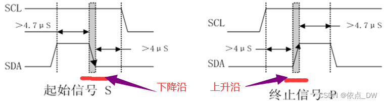
Starting conditions
It can be known from the sequence diagram ,SCL and SDA It is high level by default , At the same time, it needs to be delayed 4.7us above , I give it 5us Delay of , After the SDA Pull it down , Further delay 5us, At the same time SCL Pull it down , Then the writing of the starting condition sequence code is completed .
Pay attention here ,SDA Select output mode
// start
void I2C_Start(void){

	I2C_Mode(Out);
	SCL_High;
	SDA_High;
	delay_us(5);
	SDA_Low;
	delay_us(5);
	SCL_Low;
}
The end condition
It can be known from the sequence diagram ,SCL The default state is high ,SDA The default state is low , At the same time, it needs to be delayed 4.7us above , I give it 5us Delay of , hold SDA pull up , Further delay 5us, Then the completion of the end condition timing code .
Pay attention here ,SDA Select output mode
towards SDA Bus write : The output mode
towards SDA Bus read : The input mode
// end
void I2C_Stop(void){

	I2C_Mode(Out);
	SDA_Low;
	delay_us(5);
	SCL_High;
	delay_us(5);
	SDA_High;
}
Response and non response
Every time the master sends a byte of data to the slave , The master always needs to wait for a reply from the slave , To confirm whether the slave has successfully received the data , The clock needed by the slave to answer the host is still provided by the host , The response appears every time the host completes 8 The clock period immediately following the data bit transmission , Low level 0 To answer ,1 It means no response .
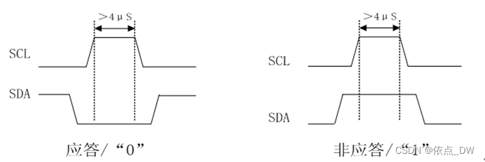
It can be known from the sequence diagram , No matter in the answer state , Or in the non response state ,SCL It's all high level , Well, first put SCL pull up , Then delay 4us, To determine SDA The state of ;
Define a Time Variable , If you don't answer , Both read SDA Data bits for 1, Just send a stop signal , Indicates that the device does not exist , Prevent the program from stopping stuck in this position , Then a non reply signal is returned 1;
If you read SDA Data bits for 0, To answer , Then put SCL Pull it down , Time delay 4us, Finally back to 0, It completes an operation of answering .
// Answer non answer judgment
u8 I2C_Write_Ack(void){

	u8 Time;
	I2C_Mode(Input);
	SCL_High;
	delay_us(4);


		while(GPIO_ReadInputDataBit(I2C_PROT,SDA)){

			if(++Time>250){

				I2C_Stop();
				return 1;//1  Non response
			}
		}
		SDA_Low;//0  The reply
		delay_us(4);


	return 0;
}
The validity of the data
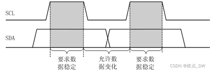
stay Writing data when , When SCL Low power level , Allow data to change , At this time, you can write data . that , How to operate ? First of all, we need to put SCL Pull it down , And then keep 4us; Then select the output mode , Then start from the high position bit One bit Writing data .
Be careful :I2C Write data from the high order .
// Write Bytes
void I2C_Write_Byte(u8 data){

	SCL_Low;
	delay_us(4);
	for(u8 i=0;i<8;i++){

		I2C_Mode(Out);

		if((data<<i)&0x80) SDA_High;
		else
		SDA_Low;

		SCL_High;
		delay_us(4);
		SCL_Low;
		delay_us(4);
	}
}
stay Reading data when , Select input mode , We need to SCL Bus up , Because at this time, the data is stable and effective , After reading the SDA The data of , If SDA High level ,data Or on the 0x01, After reading the data , take SCL Pull it down , Finally back to data.
data<<=1;// Read data from the low order , Keep moving left , Low will become high .
// Reading data
u8 I2C_Read_Data(void){

	u8 data;

	for(u8 i=0;i<8;i++){

		I2C_Mode(Input);
		SCL_High;
		delay_us(4);
		data<<=1;

		if(GPIO_ReadInputDataBit(I2C_PROT,SDA) == SET){

			data |= 0x01;
		}
		SCL_Low;
		delay_us(4);
	}
	return data;
}
Since then , All the three parts of the code have been written , After we understand the principle and usage of these three sequences , Next, I will tell you how to drive on this basis I2C Interface OLED.
OLED brief introduction
2. communication interface : 3-wire SPI, 4-wire SPI, I2C
3. Screen type : OLED
4. Control chip : SSD1306
5. The resolution of the : 128*64(Pixel)
6. Dimensions : 128*64(Pixel)
7. Display color : Yellow blue ( Two color block screen )
8. working temperature : -20°C ~ 70°C
9. Storage temperature : -30°C ~ 80°C
10. visual angle : >160
matters needing attention :OLED The display is different from LCD,OLED Power on is unresponsive , You need a driver to display !
Wiring way :
SDA --- PC0
SCL --- PC1
VCC --- 5V
GND --- The earth
OLED Communication address and register address
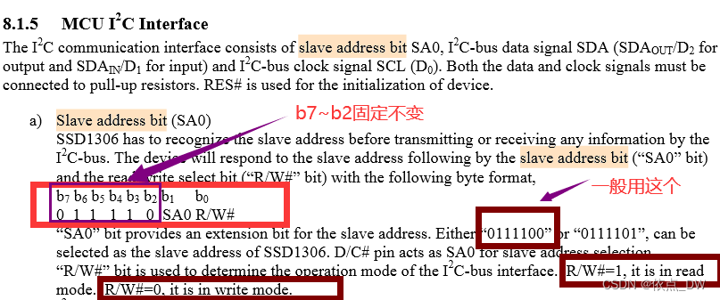
be-all I2C Devices will have hardware addresses , That is, the address of the chip , You can know from the manual ,b7~b2 Is fixed ,b1(SA0) General choice 0,bo(R/W) Used to determine the I2C Operation mode of general interface ,R/w # = 1, It is in read mode .R/w # = 0, It is in write mode . Generally only to OLED Writing data , Therefore, its address is :0111 1000(0x78) , So we define OLED The device address is
#define OLED 0X78
0x78: Write device address
Bus sequence diagram

We can know from the bus sequence diagram , The process of sending data or commands is as follows :

According to the above steps , The code we write is as follows :
void OLED_Write_Cmd_Data(u8 cmd,u8 data){

	I2C_Start();
	I2C_Write_Byte(OLED);
	I2C_Write_Ack();


	if(!cmd){
	I2C_Write_Byte(0X00);
	I2C_Write_Ack();
	I2C_Write_Byte(data);
	}
	else{
	I2C_Write_Byte(0X40);
	I2C_Write_Ack();
	I2C_Write_Byte(data);
	}
	I2C_Write_Ack();
	I2C_Stop();
}
0: Write orders
1: Writing data
thus , The most important part of the code has been written , Other things about OLED The description of has been detailed and clear in the ninth article :
9.[STM32]0.96 " OLED Hard to understand ? Take a look at this . Well, let's see the effect !

In order to facilitate the next search , Remember to pay a little attention .
This chapter ends , I'll see you in the next chapter
Reference material :
1.STM32 Firmware library manual
2. The punctual atoms STM32 Incomplete manual _ Library function version
3. Reference video Reference article 9.[STM32]0.96 " OLED Hard to understand ? Take a look at this
Data uploaded , You need to take it yourself
边栏推荐
- SQL Server learning notes
- Optional parameters in the for loop
- 1330: [example 8.3] minimum steps
- Interval DP (gravel consolidation)
- JS topic - console log()
- Bugku's Ping
- Lesson 4 knowledge summary
- 【 note 】 résoudre l'erreur de code IDE golang
- Reproduce ThinkPHP 2 X Arbitrary Code Execution Vulnerability
- Your childhood happiness was contracted by it
猜你喜欢

Example of lvgl display picture
Data communication foundation - dynamic routing protocol rip
Optional parameters in the for loop
![17.[STM32]仅用三根线带你驱动LCD1602液晶](/img/c6/b56c54da2553a451b526179f8b5867.png)
17.[STM32]仅用三根线带你驱动LCD1602液晶

Appium自动化测试基础 — APPium基础操作API(二)
Common MySQL interview questions
Appium automation test foundation - appium basic operation API (II)

一文搞定vscode编写go程序

D-snow halo solution
Bubble sort, insert sort
随机推荐
F. Min cost string problem solving Report
Arduino controls a tiny hexapod 3D printing robot
episodic和batch的定义
SQL injection sqllabs (basic challenges) 1-10
Optional parameters in the for loop
CODING DevSecOps 助力金融企业跑出数字加速度
通过的英特尔Evo 3.0整机认证到底有多难?忆联科技告诉你
17.[STM32]仅用三根线带你驱动LCD1602液晶
Where is the operation of convertible bond renewal? Is it safer and more reliable to open an account
Misc Basic test method and knowledge points of CTF
Severlet learning foundation
Huiyuan, 30, is going to have a new owner
Install PHP extension spoole
Go learning ----- relevant knowledge of JWT
数学建模之层次分析法(含MATLAB代码)
Verilog realizes the calculation of the maximum common divisor and the minimum common multiple
Appium自动化测试基础 — APPium基础操作API(一)
Ten billion massage machine blue ocean, difficult to be a giant
Au - delà du PARM! La maîtrise de l'Université de Pékin propose diverse pour actualiser complètement le classement du raisonnement du NLP
CSRF, XSS science popularization and defense