当前位置:网站首页>Characteristics and electrical parameters of DDR4
Characteristics and electrical parameters of DDR4
2022-07-05 11:02:00 【ltqshs】
DDR4 What are the characteristics ?
DDR Series have DDR,DDR2、DDR3、DDR4、DDR2L、DDR3L、DDR4L、 And the latest DDR5. Although technology is improving , But there are many similarities between each generation . Let's observe DDR Features of mainstream series products , It is not difficult to find rules .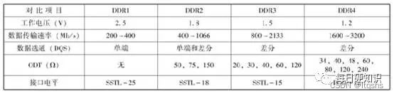
Obviously , The voltage is getting lower and lower , The frequency is getting higher and higher , The data bus has developed from single ended to differential . We found that this is similar to the development history of the bus .
The root of science and technology is still the most common wisdom of mankind , Don't believe it ? Let's take an inappropriate plum , chestnuts , Example .
If there are many plums on this side of the river , There are many chestnuts across the river , If only manpower , Carry the chestnuts across the river and the plums here back and forth as soon as possible , What methods do you have ? You can easily come up with several solutions , Find more people to move at the same time ; Find a brother who swims fast ; Move where the river is narrow ;2 A group of people ,A Throw plums ,B Throw chestnuts ….
You think you are , Smart predecessors are just like you , This kind of thinking is applied to DDR On the design of .
At first, I found many people to move together , therefore DDR At first, parallel routing design ; Later, I looked for someone who could swim fast , therefore DDR The frequency of is increasing ; Swimming is fast but tired , We have to find a narrow place to swim , therefore DDR The working level is getting lower and lower ( The current transmission speed is certain , So the lower the voltage , The less time it takes ). It's not a thing to swim back and forth all the time , Can two people form a group , You are responsible for moving 0, I'm in charge of moving 1, therefore DDR The bus is gradually evolving from parallel to differential .
That's it DDR The law of technological development , It is also the development law of many buses . Grasp the law , Let's look at features ,DDR4 level 1.2V,DQS The signal is differential , Frequency at 1600Mbps~3200Mbps.
DDR4 What are the key signals ?
DDR4 What are the key signals ? A picture can be seen . Yes CK,ADDR,DQS,DQ,DQM The signal , Outside the circuit , You can also see enabling , Reset ,ODT,ZQ.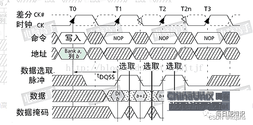
So what are the functions of these signals ? Let's make a brief introduction next .
1. CK,Address,DQS,DQ,DM What are the functions of signals ?
CK yes DDR Data communication clock signal of , When CK and Address When the signal works together , Can be done CMD( command ) Operation and Address( Address ) Signal transmission . Because the address signal and command signal are in DDR The operation process belongs to the control signal , relative DDR Data transmission of , It belongs to a niche scene , therefore DDR Address signal and CMD The signal is still single ended , The working frequency is also lower than that of data transmission . So it's not hard for us to find out ,ADDR The signal is still single ended , And most of the matching resistors are still external .
Because data transmission is DDR Main business of , So in DDR Data transfer , Additional measures are needed to ensure data transmission , therefore DDR4 Added new roles ,DQS,DQ,DM The signal .
Data selection pulse (DQS) yes DDR The important function of , Its function is mainly used to accurately distinguish each transmission cycle in a clock cycle , And facilitate the receiver to accurately receive data . Every chip has a DQS The signal line , It's two-way , When writing, it is used to transfer CPU It's from DQS The signal , When reading , By DDR Generate DQS towards CPU send out . It can be said that , It is the synchronization signal of data . You can even say that ,CK and DQS coordinate , As DQ Reference clock of data line , This is also why when wiring ,DQS and DQ Reasons to consider together .
In the process of continuous data transmission , As the clock changes ,CPU You may read DDR Middle position 1, Location 2, Location 3, Location 4 The data of , Suppose in this continuous transmission process ,CPU Don't want position 2 The data of , Don't want to interrupt data transmission , So what can I do ?DQM That comes in handy , At transfer to location 2 yes ,DQM Can make , You can shield the position 2 The data of .
2. What is? ODT?
The chip terminal is terminated with matching resistance On-Die Termination Referred to as ODT.ODT It's from DDR2 Later products began to appear , And with the upgrading of products ,ODT Present more values . At present ,ODT Mainly used for data (data,DQ)、 Data gating (DQS/DQS#) And data mask (Data Mask,DM) Three types of signal lines .ODT Its function is to replace the conventional circuit matching design , The discrete termination resistors originally outside the chip are integrated into the chip , The simplified circuit structure is shown in the figure below .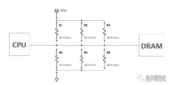
ODT Introduction of circuit , yes DDR Milestones of development ,ODT It has the following advantages .
Removed PCB Discrete terminating resistor elements on the board , Reduce the cost of hardware design .
Since there is no termination resistance , send PCB The design has more wiring space , convenient EDA wiring .
because ODT Adjust through the internal register , It can be turned on and off by software , Reduce the debugging workload .
Chip internal termination is more effective than board level termination , There are not too many parasitic effects .
Reduce the number of external components , The reliability is also optimized .
ODT The introduction of , To further improve DDRx The working frequency of the memory is paved .
Of course ,ODT Not all are advantages , Because of the use of ODT, The type and value of matching resistance have been determined and cannot be modified ; To some extent, it will also bring a certain increase in power consumption , Therefore, some consumer products are not always open ODT function .
3. What is? ZQ calibration ?
ZQ yes DDR3 Then add a new pin , and DDR3 It is through ZQ Conduct output resistance (Ron) and ODT Calibration of , This calibration process is in DRAM The initialization process will be completed .ZQ It is relatively simple in principle design ,ZQ The pin passes a low tolerance 240Ω( The general tolerance is 1%) The resistance of is directly connected to the ground .
Except eye chart ,DDR4 Also look at those electrical parameters ?
DDR4 Whether the design is designed OK, You need to see DDR4 Whether the measured parameters of meet JEDEC standard . What electrical parameters are defined in the specification ? What meaning does each electrical parameter represent ? Next we will make a brief introduction .
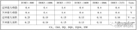
1. Overshoot and undershoot .
If the impedance of the signal is discontinuous during transmission , There will be reflection , Reflection is shown on oscilloscope waveform , It's the signal up and down , stay DDR During the design process , We are not concerned with the overshoot amplitude of the signal at a certain point in time , But the integral of overshoot in the time dimension . Focus on a process , Not a point .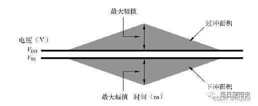
For each signal , The protocol specifications will be here 4 Define and standardize signal integrity in three dimensions .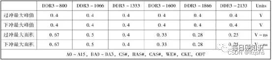
2. High and low levels of the signal .
In high-speed signal transmission , Whether the signal can reach the minimum threshold of high level and the maximum threshold of low level specified in the Protocol , It also directly determines the stability of the product .
stay DDR Specification , Single ended address and control commands 、 Single ended data and data mask signals AC and DC Input level , Differential clock and data strobe signal AC and DC The input level will be clearly defined . During simulation and testing , We only need to pay attention to whether the measured value in a specific scenario reaches the value specified in the agreement .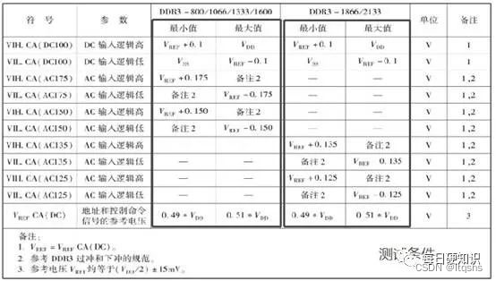
3. Differential signal intersection voltage .
In order to meet the signal establishment and holding time , The single ended intersection of differential signal must be within a certain range .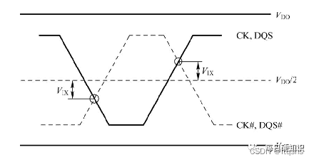
The intersection is marked with V DD/2 As a reference voltage , The measurement is relative to V DD/2 The deviation of , The smaller the deviation, the better .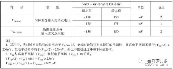
4. Timing requirements .
The main requirements of time order relationship are 3 Group : Address 、 Between control and command signals and clock signals ; Between data strobe signal and clock signal ; data 、 Between data mask and data strobe . So in PCB When the design , It is also designed in groups according to signals , Address 、 Control and command signals are grouped with clock signals , data 、 Each byte of data mask signal and data strobe signal is a group , The signals of the same group will basically keep the length difference within a certain range during design , And the design method is basically the same ( As if the group wiring is on the same floor 、 Have the same number of vias ), Only in this way can we meet the requirements of timing .
5. Slope derating .
There are two ways to measure the slope in the specification of the bus , They are the conventional measurement method and the tangent measurement method , By address 、 Take control and command signals for example , Its definition is shown in the figure below .
These two measurement methods are mainly determined by the quality of the waveform obtained , If the monotonicity of the waveform is better , Then measure in a conventional way ; If monotonicity is not good , There are some hooks or steps , Then use tangent method to measure .
The red box in the figure represents the conventional slope measurement method , The green arrow represents the tangent measurement method . stay DDR in , The establishment and holding time of the signal is not the only constant , It will change as the slope changes , To compensate for the effect of slope , In the simulation of the final “ Build and maintain time ” when , The measured timing parameters need to be added to the derating parameters . Derating parameters and signal slope and clock / The slope of data gating .
Reference to the original :《DDR4 Practical teaching ( 3、 ... and ): Characteristics and electrical parameters 》
边栏推荐
猜你喜欢
32:第三章:开发通行证服务:15:浏览器存储介质,简介;(cookie,Session Storage,Local Storage)

2022年化工自动化控制仪表考试试题及在线模拟考试

go语言学习笔记-初识Go语言
Go语言-1-开发环境配置
微信核酸检测预约小程序系统毕业设计毕设(8)毕业设计论文模板
【js学习笔记五十四】BFC方式
关于vray 5.2的使用(自研笔记)(二)
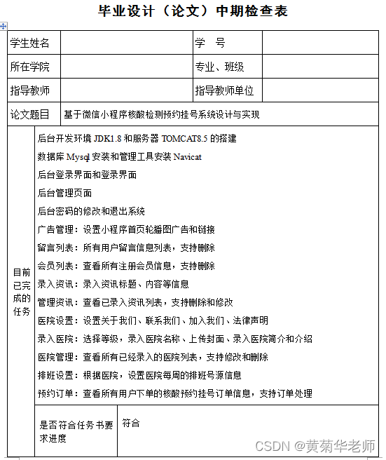
Wechat nucleic acid detection appointment applet system graduation design completion (7) Interim inspection report
About the use of Vray 5.2 (self research notes) (II)
32: Chapter 3: development of pass service: 15: Browser storage media, introduction; (cookie,Session Storage,Local Storage)
随机推荐
Applet framework taro
Go-3-the first go program
Go-3-第一个Go程序
函数///
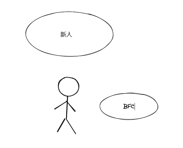
【js学习笔记五十四】BFC方式
中职组网络安全2021年江苏省省赛题目5套题目环境+解析全有需要的私信我
32: Chapter 3: development of pass service: 15: Browser storage media, introduction; (cookie,Session Storage,Local Storage)
C语言活期储蓄账户管理系统
Sqlserver regularly backup database and regularly kill database deadlock solution
变量///
小红书自研KV存储架构如何实现万亿量级存储与跨云多活
BOM//
Nine degrees 1480: maximum ascending subsequence sum (dynamic programming idea for the maximum value)
DGL中的消息传递相关内容的讲解
Msfconsole command encyclopedia and instructions
基于昇腾AI丨爱笔智能推出银行网点数字化解决方案,实现从总部到网点的信息数字化全覆盖
基于OpenHarmony的智能金属探测器
Use bat command to launch common browsers with one click
DDR4的特性与电气参数
String