当前位置:网站首页>On boost circuit
On boost circuit
2022-07-05 08:09:00 【Learning notes of hardware Xiaobai】
BOOST circuit , As a hardware engineer, I am familiar with a hardware circuit that I can no longer be familiar with . It will be used in many hardware fields .
Take Xiaobai's mobile phone / Tablet field , It also uses many and BOOST Related modular design . For example, the backlight module of the screen , Audio amplifier SMART PA Module and flash drive module, etc . Although different IC, But it is still BOOST Extended design of circuit . As long as you are familiar with BOOST Relevant knowledge , You can easily understand the design principle of these modules . Even in the face of strange boost module circuit related IC, You can also skillfully build its peripheral circuit .
Said so much , Next, let's move on to our topic -BOOST circuit .
First , First map .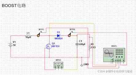
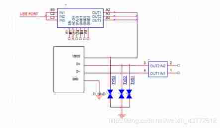
The picture shows the simplest BOOST Circuit diagram of boost circuit . It mainly includes power supply V1, Schottky diode D1, Power inductance L1, as well as NMOS tube Q1 And capacitance C1, load R1.
among ,MOS The source of the tube is grounded , The grid is connected to a certain frequency PWM wave .
Read about MOS Everyone knows ,MOS Tubes are voltage driven devices . Just give G A certain voltage makes GS There is a certain pressure difference between , Satisfy VGS>VGS(th) Can make MOS The tube is in the conduction state .PWM As a square wave of a certain frequency , Its level fluctuates .
When G Extremely high electricity , here MOS The pipe is open , Ignore DS In case of pressure drop , It can be regarded as a wire .
When G Extremely low electricity level , here MOS The tube is closed , It can be regarded as an open circuit .
PWM High and low levels constantly change , That's why MOS The branch where the pipe is located , Keep on and off . As long as the frequency of on and off is large enough , It can output a stable voltage .
Discuss this circuit , I will discuss the following two scenarios .
(1)MOS The tube goes from closed to on : The current flow of the circuit is :V1 Positive pole →L1→V1 Negative pole . Almost all of the power supply is supplied by inductors L1, Inductance for energy storage . Parallel with the load at the same time C1 Discharge at this stage ,C1 The voltage at both ends shall not change suddenly .D1 The existence of , Prevented C1 Ground discharge .
(2)MOS The tube goes from on to off : The current flow of the circuit is :V1 Positive pole →L1→D1→R1→V1 Negative pole . Because the inductance belongs to the energy storage element , And it has the reason why the current cannot change suddenly , So at this time, the current flowing through the inductance , Still keep and MOS Direction of pipe conduction , And in the disconnected state , Inductance releases energy to the outside .
In order to better understand its role in boosting , We can simply compare inductance to a battery . stay MOS When the pipe is disconnected , The internal current of the battery flows from the negative pole → Positive pole , The external current is from the positive pole → Negative pole . So both ends of the inductance , The left end is regarded as the negative pole , The right end is positive . It just coincides with V1 Series connection , It is equivalent to two batteries in series , Its combined action gives the load R1 Transfer energy . At this time, the voltage of the load resistance must be greater than the input voltage V1, Therefore, the purpose of boosting is achieved .
BOOST The principle of boosting , We know . The reason is MOS The conduction and closure of the tube work together to produce . Understand the principle , Still can't forget the calculation of the output voltage value , Which parameters are strongly related .
The second volt theorem of voltage balance exists in inductance . In switching power supply , That is, the voltage applied to both ends of the inductor multiplied by the on time is equal to the voltage at both ends of the inductor multiplied by the off time at the off time . In this circuit , Ignore MOS Under ideal conditions such as tube voltage drop and Schott diode voltage drop .
Conduction time , The voltage across the inductor is Vin, Conduction time DT.
closed , The voltage across the inductor is Vo-Vin, Closing time is (1-D)T.
therefore VinDT=(Vo-Vin)(1-D)T.
Vo=VinD /(1-D) +Vin
Vo=Vin/(1-D)
therefore , We can see that the output voltage value mainly depends on the input voltage value and PWM The duty cycle of . among , When the duty cycle is 50% when , The output voltage is twice the input voltage .
Finished talking about the output voltage , Then let's talk about another physical quantity worthy of attention - Inductive current , It requires a formula UL=L*di /dt.
According to the formula, we can deduce , Inductance current value I It is proportional to time and inversely proportional to inductance . therefore , When we use an oscilloscope to measure the current waveform flowing through the inductor , You will find that it is a straight line with a certain slope , Instead of our common horizontal straight line . among ,MOS When the pipe is on and off , The polarity of the inductance will be reversed , So see the complete current waveform , It should belong to the shape of discount ,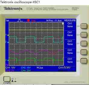
Therefore, there are simulation circuit diagrams , The pink waveform in the oscilloscope . The selection of inductance is also very important , Its sensing value and saturation current are worthy of attention . How to choose , This is not what today's article will discuss , I'll do a special push later .
BOOST Circuit as a very important knowledge , As a hardware engineer should understand the circuit . Xiaobai described it in a concise way , I hope you can understand .
边栏推荐
- WiFi wpa_ Detailed description of supplicant hostpad interface
- Halcon's practice based on shape template matching [1]
- Record the visual shock of the Winter Olympics and the introduction of the screen 2
- [trio basic tutorial 16 from introduction to proficiency] UDP communication test supplement
- Define in and define out
- Verilog -- state machine coding method
- 2021-10-28
- Consul安装
- solver. Learning notes of prototxt file parameters
- How to excavate and research ideas from the paper
猜你喜欢
The firmware of the connected j-link does not support the following memory access

C language enhancement -- pointer

Consul安装
H264 (I) i/p/b frame gop/idr/ and other parameters
![C WinForm [help interface - send email] - practice five](/img/2a/c4e7abe054e6fdd45acc7d297a033d.jpg)
C WinForm [help interface - send email] - practice five

UEFI development learning 5 - simple use of protocol
![C WinForm [display real-time time in the status bar] - practical exercise 1](/img/9f/d193cbb488542cc4c439efd79c4963.jpg)
C WinForm [display real-time time in the status bar] - practical exercise 1
Talk about the circuit use of TVs tube

Network port usage
Record the visual shock of the Winter Olympics and the introduction of the screen 2
随机推荐
Imx6ull bare metal development learning 1-assembly lit LED
Some tips for using source insight (solve the problem of selecting all)
Live555 RTSP audio and video streaming summary (II) modify RTSP server streaming URL address
[popular science] some interesting things that I don't know whether they are useful or not
Basic embedded concepts
Several implementation schemes of anti reverse connection protection of positive and negative poles of power supply!
Arduino uses nrf24l01+ communication
PMSM dead time compensation
1-stm32 operation environment construction
Train your dataset with yolov4
Why is 1900 not a leap year
Markdown tips
Communication standard -- communication protocol
Step motor generates S-curve upper computer
UEFI development learning 3 - create UEFI program
Talk about the function of magnetic beads in circuits
Anonymous structure in C language
After installing the new version of keil5 or upgrading the JLINK firmware, you will always be prompted about the firmware update
Correlation based template matching based on Halcon learning [II] find_ ncc_ model_ defocused_ precision. hdev
Slist of linked list