当前位置:网站首页>Learning record: STM32F103 clock system overview working principle
Learning record: STM32F103 clock system overview working principle
2022-07-06 15:32:00 【Bitter tea seeds】
Catalog
One 、 Look at the clock tree below, we can find STM32 Yes 5 A clock source
Two 、 STM32F103 Clock system configuration
Preface
If you want to use a single-chip microcomputer well, you must know the principle of the microcontroller , So when applying it , Can be handy to understand how it works . When something goes wrong with the project , You can also find the source and solution of the problem at the bottom .STM32 The clock system is better than 51 The clock system of single chip microcomputer is much more complicated , After all 51 SCM has only one clock system .
from STM32 Refer to the manual , I have learned that STM32F103MCU There are three different clock sources that can be used to drive the system clock (SYSCLK): HSI Oscillator clock 、HSE Oscillator clock 、PLL The clock . When not used , Any clock source can be turned on or off independently , Thus, the system power consumption is optimized .
So I can know , STM32 The purpose of adopting multiple clock sources is to reduce the power consumption of the clock , In digital electronic technology : The same circuit , The faster the clock, the more power it consumes , And the ability to resist electromagnetic interference is weaker , The more unstable the pulse is .
One 、 Look at the clock tree below, we can find STM32 Yes 5 A clock source
( Refer to the development guide of punctual atom )
ⅰ、HSI yes High speed internal clock ,RC oscillator ( stay Multisim In the column , The circuit of Wen's bridge is simulated , If you want to know more about it, you can go and have a look ), The frequency is 8MHz.
ⅱ、HSE yes High speed external clock , It can be connected to quartz / Ceramic resonator ( stay Multisim In the column , The quartz crystal circuit is simulated , If you want to know more about it, you can go and have a look ), Or connect to the external clock source , The frequency range is 4MHz~16MHz.
ⅲ、LSI yes Low speed internal clock ,RC oscillator , The frequency is 40kHz. The clock source of the independent watchdog can only be LSI, Same as when LSI It can also be used as RTC The clock source of .
ⅳ、LSE yes Low speed external clock , The connection frequency is 32.768kHz Quartz crystal . This is mainly RTC The clock source of .
ⅴ、PLL by PLL frequency doubling output , Its clock input source can be selected as HSI/2、HSE perhaps HSE/2. Frequency doubling can be selected as 2~16 times , But the maximum output frequency shall not exceed 72MHz.
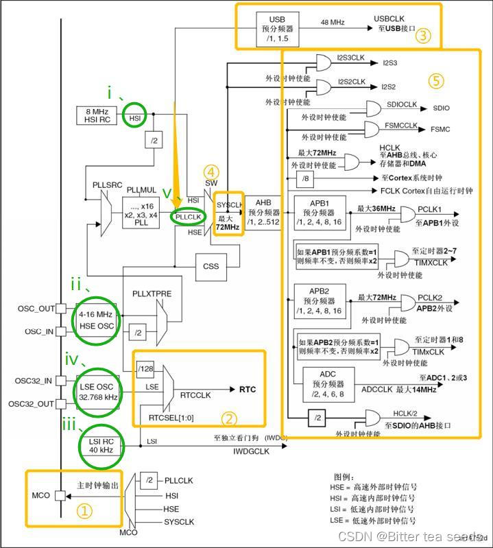
①、MCO yes STM32 A clock output of IO(PA8), It can select a clock signal output , You can choose PLL Output 2 frequency division 、HSI、HSE Or the system clock . This clock can be used to provide clock source for other external systems .
②、 Here is RTC Clock source , As you can see from the diagram ,RTC The clock source can be selected LSI,LSE, as well as HSE Of 128 frequency division .
③、 As you can see from the diagram USB The clock is from PLL Clock source .STM32 There is a full speed function in Of USB modular , Its serial interface engine needs a frequency of 48MHz The clock source of . The clock source can only come from PLL Output access , You can choose 1.5 Divide the frequency or 1 frequency division , That is to say , When needed USB When the module ,PLL Must enable , And the clock frequency is configured as 48MHz or 72MHz.
④、 STM32 System clock SYSCLK, It's for STM32 Most of the components work in the clock source . The system clock can be selected as PLL Output 、HSI perhaps HSE. The maximum frequency of the system clock is 72MHz, Of course, you can also overclock , However, in general, there is no need to risk overclocking for the sake of system stability .
⑤、 It refers to all other peripherals . As can be seen from the clock chart , The ultimate source of clocks for all other peripherals is SYSCLK.SYSCLK adopt AHB After the frequency divider is divided, it is sent to each module for use . These modules include :
1、AHB Bus 、 kernel 、 Memory and DMA The use of HCLK The clock .
2、 adopt 8 After frequency division Cortex System timer clock , That is to say systick .
3、 Give directly to Cortex Idle running clock FCLK.
4、 Send APB1 Frequency divider .APB1 The frequency divider outputs one circuit for APB1 Peripheral use (PCLK1, Maximum frequency 36MHz), The other way to the timer (Timer)2、3、4 Frequency multiplier use .
5、 Send APB2 Frequency divider .APB2 The frequency divider outputs one channel for APB2 Peripheral use (PCLK2: Maximum frequency 72MHz), The other way to the timer (Timer)1 Frequency multiplier use .
APB1 The above is connected with low-speed peripherals , Including power interface 、 Backup interface 、CAN、USB、I2C1、I2C2、UART2、UART3 wait ,APB2 The high-speed peripheral package is connected above enclosed UART1、SPI1、Timer1、ADC1、ADC2、 All ordinary IO mouth (PA~PE)、 Second function IO Mouth, etc .
Two 、 STM32F103 Clock system configuration
( Are all based on STM32 Register for programming )
typedef struct /* register */
{
__IO uint32_t CR; //HSI,HSE,CSS,PLL Wait for the enable and ready flag bits
__IO uint32_t CFGR; //PLL Wait for the clock source selection , Frequency division coefficient setting
__IO uint32_t CIR; // eliminate / Can make Clock ready interrupt
__IO uint32_t APB2RSTR; //APB2 On line peripheral reset register
__IO uint32_t APB1RSTR; //APB1 On line peripheral reset register
__IO uint32_t AHBENR; //DMA,SDIO Wait for the clock to enable
__IO uint32_t APB2ENR; //APB2 On line peripheral clock enable
__IO uint32_t APB1ENR; //APB1 On line peripheral clock enable
__IO uint32_t BDCR; // Backup domain control register
__IO uint32_t CSR; // Control status register
} RCC_TypeDef;
1.SystemInit Initializer :
void SystemInit (void)
{
  /* Reset the RCC clock configuration to the default reset state(for debug purpose) */
  /* Set HSION bit */
  RCC->CR |= (uint32_t)0x00000001; // open  HSION  position


  /* Reset SW, HPRE, PPRE1, PPRE2, ADCPRE and MCO bits */
#ifndef STM32F10X_CL
  RCC->CFGR &= (uint32_t)0xF8FF0000;
#else
  RCC->CFGR &= (uint32_t)0xF0FF0000;
#endif /* STM32F10X_CL */

  /* Reset HSEON, CSSON and PLLON bits */
  RCC->CR &= (uint32_t)0xFEF6FFFF;//  Reset  HSEON, CSSON  and  PLLON  position


  /* Reset HSEBYP bit */
  RCC->CR &= (uint32_t)0xFFFBFFFF; //  Reset  HSEBYP  position


  /* Reset PLLSRC, PLLXTPRE, PLLMUL and USBPRE/OTGFSPRE bits */
  RCC->CFGR &= (uint32_t)0xFF80FFFF;// Reset  CFGR  register


#ifdef STM32F10X_CL
  /* Reset PLL2ON and PLL3ON bits */
  RCC->CR &= (uint32_t)0xEBFFFFFF;

  /* Disable all interrupts and clear pending bits  */
  RCC->CIR = 0x00FF0000;

  /* Reset CFGR2 register */
  RCC->CFGR2 = 0x00000000;
#elif defined (STM32F10X_LD_VL) || defined (STM32F10X_MD_VL) || (defined STM32F10X_HD_VL)
  /* Disable all interrupts and clear pending bits  */
  RCC->CIR = 0x009F0000;

  /* Reset CFGR2 register */
  RCC->CFGR2 = 0x00000000;
#else
  /* Disable all interrupts and clear pending bits  */
  RCC->CIR = 0x009F0000;
#endif /* STM32F10X_CL */

#if defined (STM32F10X_HD) || (defined STM32F10X_XL) || (defined STM32F10X_HD_VL)
  #ifdef DATA_IN_ExtSRAM
    SystemInit_ExtMemCtl();
  #endif /* DATA_IN_ExtSRAM */
#endif

  /* Configure the System clock frequency, HCLK, PCLK2 and PCLK1 prescalers */
  /* Configure the Flash Latency cycles and enable prefetch buffer */
  SetSysClock();

#ifdef VECT_TAB_SRAM
  SCB->VTOR = SRAM_BASE | VECT_TAB_OFFSET; /* Vector Table Relocation in Internal SRAM. */
#else
  SCB->VTOR = FLASH_BASE | VECT_TAB_OFFSET; /* Vector Table Relocation in Internal FLASH. */
#endif
}
SystemInit The following three aspects are mainly done : 1) Reset RCC The clock is configured as the default reset value ( It starts by default HIS) 2) External memory configuration 3) Interrupt vector table address configuration .
2.SetSysClockTo72
Set the system clock frequency to 72MHz And configuration HCLK、PCLK2 and PCLK1 Preassigned frequency counter .
Status after initialization :
SYSCLK 72MHz
AHB 72MHz
PCLK1 36MHz
PCLK2 72MHz
PLL 72MHz
After initialization, you can use the variable SystemCoreClock Get system variables . If SYSCLK=72MHz, So variable SystemCoreClock=72000000.
static void SetSysClockTo72(void)
{
  __IO uint32_t StartUpCounter = 0, HSEStatus = 0;

  /* SYSCLK, HCLK, PCLK2 and PCLK1 configuration ---------------------------*/
  /* Enable HSE */
  RCC->CR |= ((uint32_t)RCC_CR_HSEON);

  /* Wait till HSE is ready and if Time out is reached exit */
  do
  {
    HSEStatus = RCC->CR & RCC_CR_HSERDY;
    StartUpCounter++;
  } while((HSEStatus == 0) && (StartUpCounter != HSE_STARTUP_TIMEOUT));

  if ((RCC->CR & RCC_CR_HSERDY) != RESET)
  {
    HSEStatus = (uint32_t)0x01;
  }
  else
  {
    HSEStatus = (uint32_t)0x00;
  }

  if (HSEStatus == (uint32_t)0x01)
  {
    /* Enable Prefetch Buffer */
    FLASH->ACR |= FLASH_ACR_PRFTBE;

    /* Flash 2 wait state */
    FLASH->ACR &= (uint32_t)((uint32_t)~FLASH_ACR_LATENCY);
    FLASH->ACR |= (uint32_t)FLASH_ACR_LATENCY_2;


    /* HCLK = SYSCLK */
    RCC->CFGR |= (uint32_t)RCC_CFGR_HPRE_DIV1;

    /* PCLK2 = HCLK */
    RCC->CFGR |= (uint32_t)RCC_CFGR_PPRE2_DIV1;

    /* PCLK1 = HCLK */
    RCC->CFGR |= (uint32_t)RCC_CFGR_PPRE1_DIV2;//HCLK2 frequency division

#ifdef STM32F10X_CL
    /* Configure PLLs ------------------------------------------------------*/
    /* PLL2 configuration: PLL2CLK = (HSE / 5) * 8 = 40 MHz */
    /* PREDIV1 configuration: PREDIV1CLK = PLL2 / 5 = 8 MHz */

    RCC->CFGR2 &= (uint32_t)~(RCC_CFGR2_PREDIV2 | RCC_CFGR2_PLL2MUL |
                              RCC_CFGR2_PREDIV1 | RCC_CFGR2_PREDIV1SRC);
    RCC->CFGR2 |= (uint32_t)(RCC_CFGR2_PREDIV2_DIV5 | RCC_CFGR2_PLL2MUL8 |
                             RCC_CFGR2_PREDIV1SRC_PLL2 | RCC_CFGR2_PREDIV1_DIV5);

    /* Enable PLL2 */
    RCC->CR |= RCC_CR_PLL2ON;
    /* Wait till PLL2 is ready */
    while((RCC->CR & RCC_CR_PLL2RDY) == 0)
    {
    }


    /* PLL configuration: PLLCLK = PREDIV1 * 9 = 72 MHz */
    RCC->CFGR &= (uint32_t)~(RCC_CFGR_PLLXTPRE | RCC_CFGR_PLLSRC | RCC_CFGR_PLLMULL);
    RCC->CFGR |= (uint32_t)(RCC_CFGR_PLLXTPRE_PREDIV1 | RCC_CFGR_PLLSRC_PREDIV1 |
                            RCC_CFGR_PLLMULL9);
#else
    /*  PLL configuration: PLLCLK = HSE * 9 = 72 MHz */
    RCC->CFGR &= (uint32_t)((uint32_t)~(RCC_CFGR_PLLSRC | RCC_CFGR_PLLXTPRE |
                                        RCC_CFGR_PLLMULL));
    RCC->CFGR |= (uint32_t)(RCC_CFGR_PLLSRC_HSE | RCC_CFGR_PLLMULL9);
#endif /* STM32F10X_CL */

    /* Enable PLL */
    RCC->CR |= RCC_CR_PLLON;

    /* Wait till PLL is ready */
    while((RCC->CR & RCC_CR_PLLRDY) == 0)
    {
    }

    /* Select PLL as system clock source */
    RCC->CFGR &= (uint32_t)((uint32_t)~(RCC_CFGR_SW));
    RCC->CFGR |= (uint32_t)RCC_CFGR_SW_PLL;

    /* Wait till PLL is used as system clock source */
    while ((RCC->CFGR & (uint32_t)RCC_CFGR_SWS) != (uint32_t)0x08)
    {
    }
  }
  else
  { /* If HSE fails to start-up, the application will have wrong clock
         configuration. User can add here some code to deal with this error */
  }
}
SetSysClockTo72 Set the system clock frequency to 72MHz And configuration HCLK、PCLK2 and PCLK1 Preassigned frequency counter .
Mainly through query STM32 Chinese Reference Manual , Find the corresponding register , Understand the role of each code .
边栏推荐
- Iterators and generators
- Introduction to variable parameters
- Mysql database (IV) transactions and functions
- Take you to use wxpy to create your own chat robot (plus wechat interface basic data visualization)
- ucorelab3
- 接口测试面试题及参考答案,轻松拿捏面试官
- JS --- detailed explanation of JS DOM (IV)
- 安全测试入门介绍
- How to rename multiple folders and add unified new content to folder names
- What are the software testing methods? Show you something different
猜你喜欢


随机推荐
Learning record: Tim - capacitive key detection
UCORE LaB6 scheduler experiment report
Stm32 dossiers d'apprentissage: saisie des applications
Research Report on medical toilet industry - market status analysis and development prospect forecast
软件测试方法有哪些?带你看点不一样的东西
ucorelab4
JS --- detailed explanation of JS DOM (IV)
全网最详细的postman接口测试教程,一篇文章满足你
Should wildcard import be avoided- Should wildcard import be avoided?
Your wechat nickname may be betraying you
FSM and I2C experiment report
How to rename multiple folders and add unified new content to folder names
Cadence physical library lef file syntax learning [continuous update]
ucore lab 6
Medical colposcope Industry Research Report - market status analysis and development prospect forecast
ucorelab3
C4D quick start tutorial - creating models
STM32學習記錄:輸入捕獲應用
学习记录:串口通信和遇到的错误解决方法
自动化测试中敏捷测试怎么做?