当前位置:网站首页>[quick start of Digital IC Verification] 2. Through an example of SOC project, understand the architecture of SOC and explore the design process of digital system
[quick start of Digital IC Verification] 2. Through an example of SOC project, understand the architecture of SOC and explore the design process of digital system
2022-07-05 20:30:00 【luoganttcc】
Reading guide : The author has the honor to be a pioneer in the field of electronic information in China “ University of electronic technology ” During postgraduate study , Touch the cutting edge Numbers IC Verification knowledge , I heard something like Huawei Hisilicon 、 Tsinghua purple light 、 MediaTek technology And other top IC related enterprises in the industry , Pairs of numbers IC Verify some knowledge accumulation and learning experience . Want to get started for help IC Verified friends , After one or two thoughts , This column is specially opened , In order to spend the shortest time , Take the least detours , Most learned IC Verify technical knowledge .
List of articles
- One 、SoC Architecture diagram : Core functions and design objectives
- Two 、SoC Architecture diagram : sketch SoC Functions and application scenarios
- 3、 ... and 、SoC Architecture diagram :IP Bus address mapping
- Four 、SoC Architecture diagram :Pin-MUX & PAD
- 5、 ... and 、SoC Architecture diagram : Layout Floorplan
- 6、 ... and 、SoC Architecture diagram : Territory layout - GDSII
- 6、 ... and 、SoC Architecture diagram :Pin & Supply voltage
- 7、 ... and 、 Digital system design node (SoC Design Node)
- Reference resources
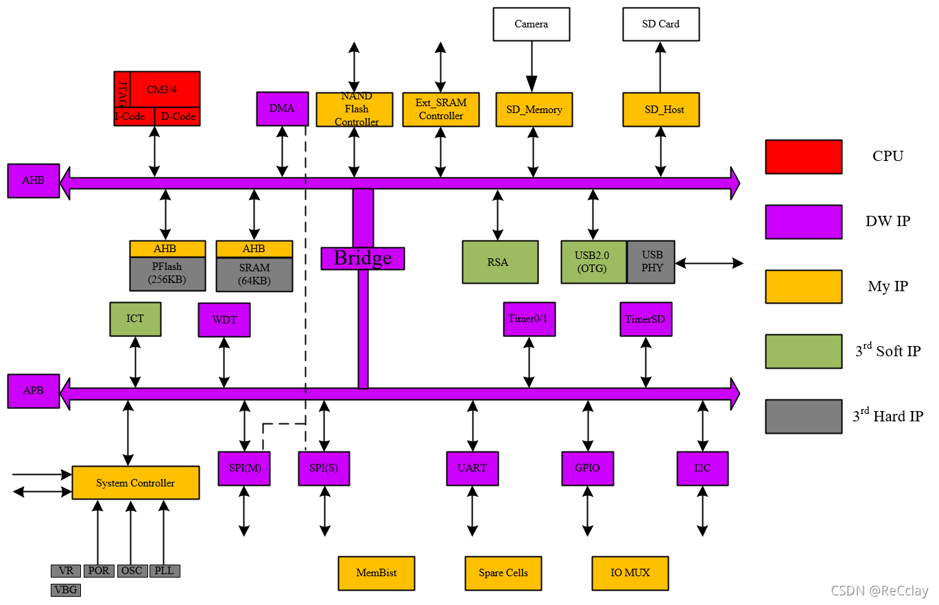
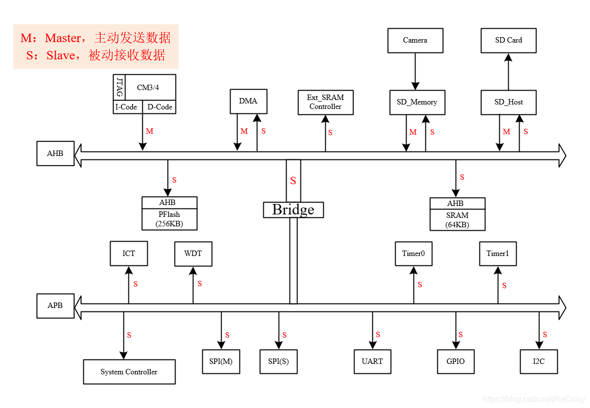
One 、SoC framework chart : Core functions and design objectives
SoC It is designed based on the idea of general processor , And PC The design idea is the same . That is, the general-purpose processor is composed of CORE + MEM Two parts , Modify the software to achieve different functions , The computer is the same computer , The hardware composition is the same .
SoC The four components of the architecture diagram :
- 1、 nucleus CORE
- 2、 Storage MEM
- 3、 peripherals IO
- 4、 Bus BUS
SoC The overall architecture is as follows :
1.1、SoC - nucleus CORE
For nuclear , Now there are three kinds of mainstream cores :
- CISC(Complex Instruction Set Computer - Complex instruction set computer )
- x86 As a representative , Company has AMD and INTEL,PC and Server More such nuclei are used .
- RISC(Reduced Instruction Set Computing - Reduced instruction set computer )
- ARM As a representative , Mobile phone chip 、 Embedded systems use such cores more .
- ARM-M series : Low-end , Commonly used in micro control scenarios , Such as MCU
- ARM-R series : Middle end , Often used in real-time scenes , Such as medical devices , Routing switches
- ARM-A series : High-end , Commonly used in high-end application scenarios , Such as mobile phone chips
- ARM As a representative , Mobile phone chip 、 Embedded systems use such cores more .
- RISC-V( Open source )
- be based on ARM and x86 Between , It can be flexibly switched and assembled
- There is no mature commercial system , There is no ecological support
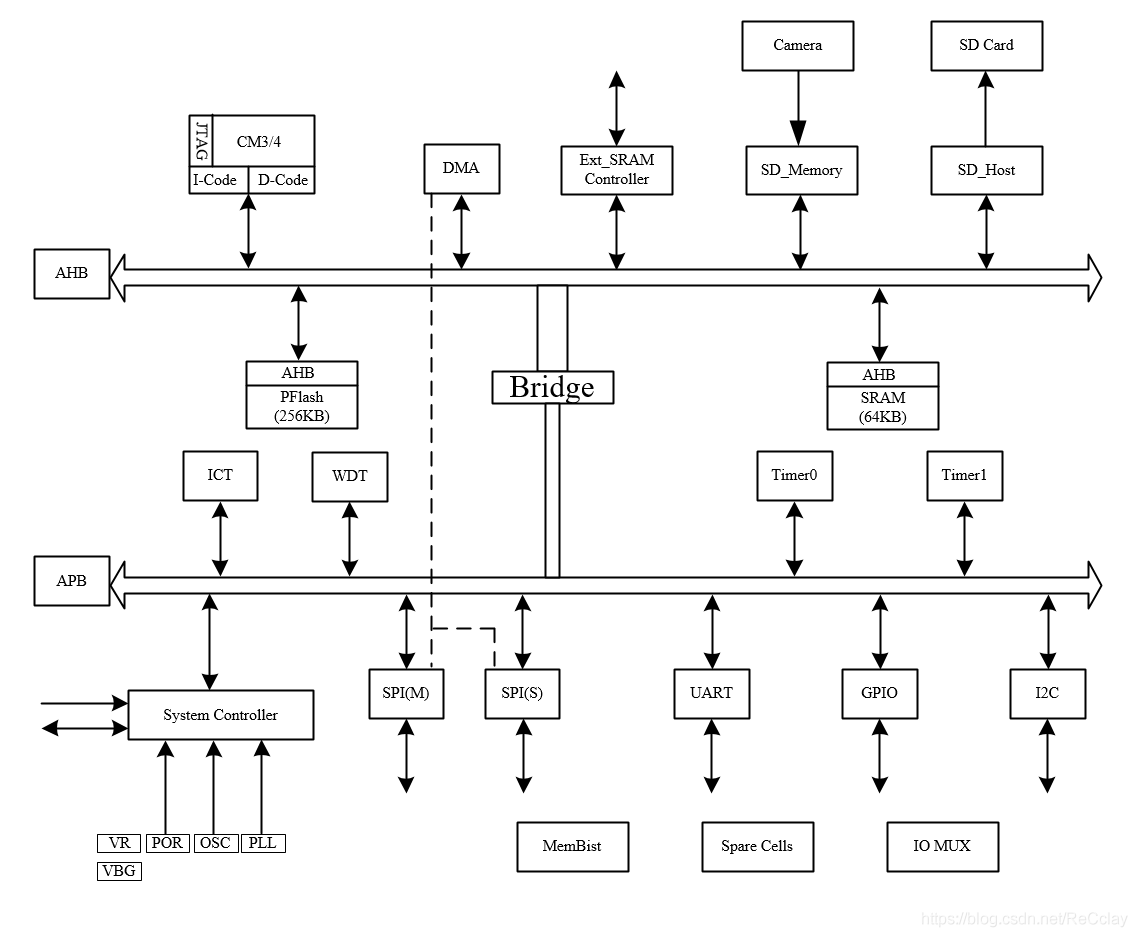
Architecture diagram , top left corner by SoC The core of the system , What is used here is ARM The company's Cortex-M3/M4 kernel .
meanwhile ,I-Code Indicates the instruction code ,D-Code Represents the data code .JTAG Used to debug chips , download debugging Program usage .
notes :
I-Code、D-CodenamelyI-Cache、D-Cache, This optional , Not every SoC They all use , According to the actual chip size and demand !
1.2、SoC - Storage MEM
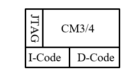
Architecture diagram , The middle part is SoC System storage , It contains PFlash and SRAM Two kinds of .
- PFlash( Hard disk ) Data in is not lost when power is off
- If PFlash Not enough use , It can be expanded Flash, Such as
NFC(Nand Flash Controller)
- If PFlash Not enough use , It can be expanded Flash, Such as
- SRAM( Memory ) The data in loses power
- SRAM It's static random access memory (Static Random Acess Memory), In contrast, there is also a dynamic random access memory (Dynamic Random Acess Memory).DRAM It needs constant refresh to keep the data ,SRAM There is no need to refresh !
- DRAM The density of is very high , So when the storage data capacity is large, it is grouped Memory The area will be smaller !SRAM Usually used in small SoC in !
- If SRAM Not enough use , It can be expanded SRAM, Like the one above
Ext_SRAM
- core After power on , Will arrive PFlash Take its instruction , To read the system to run “ Software ”( Code ), stay PFlash After starting , Download the required software to SRAM in , In the end in SRAM Running in “ Software ”.
- namely BootLoader Put it in PFlash in , Once powered on, it will load to SRAM in ,CPU Come on SRAM Take the finger to execute our program !
- SRAM The storage rate is relatively PFlash rate fast , Therefore, the program of power on running is put in SRAM in , Startup programs and unwanted data will exist PFlash in .
1.3、SoC - peripherals IO
peripherals IO In two parts :
- One is high-speed peripheral IO(AHB 100MHz):DMA、Ext_SRAM Controller、SD_Memory、SD_Host
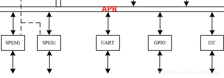
- One is low-speed peripheral IO(APB 50MHz):SPI、UART、GPIO、I2C
1.3.1、 DMA
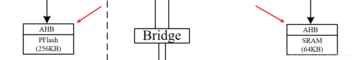
DMA(Direct Memory Access, Direct memory access ), The usage scenario is as follows : When CPU Need to move SRAM When there is a large amount of data in , If you use CPU Move , Then we will first SRAM The data in is moved to CPU In the register of , Then move to the destination by taking instructions and writing operations . This method is inefficient , And occupy CPU Valuable processing time . It's here DMA The debut of ,CPU Just tell me DMA engine , How many data you need to move from which address to which address , such DMA I went to work obediently , No longer need CPU Participation , reduce CPU The load of .
DMA There is no external interface , This can also be seen from the architecture diagram .
1.3.2、 Ext_SRAM Controller、SD_Memory And SD_Host
Ext_SRAM Controller: Usually SRAM When it's not big enough , For extended use .
Usually SD_Memory Connect a connection such as Camera The equipment , Pass the captured photo data through SD_Memory Interface stored in SRAM in , then SD_Host The interface will SRAM Save the data in to SD Card in , Take out SD Card insertion PC, You can see the photos you read !
1.3.3、 Typical low speed peripherals
Typical 3 Low speed peripheral interface :I2C、UART、SPI, The differences are as follows :
- UART It is often used for long-distance transmission , But the speed is low .
- I2C Than UART Fast speed , But the speed will not be too long ; And I2C In short distance transmission , You can pick up more than one Slave.UART It's Diandian communication ,1 individual UART The interface can only be connected to 1 individual UART Slave.1 individual I2C Master Interface , You can pick up more than one I2C Slave;
- SPI Compare with UART and I2C The speed will be higher ;1 individual SPI Master Interface , You can pick up more than one SPI Slave;SPI The amount of IO The number is also relatively I2C many !
Peripherals and CPU communicate , There are two ways :
- CPU To check our status
- Direct to CPU Send interrupt ,CPU After receiving the interrupt, I will deal with the interrupt program
BootLoader Programs and interrupt programs are written in advance , Put it in FLASH in , Once started, it will LOAD to SRAM in ! Once an interrupt occurs , It will query the interrupt program according to the interrupt vector number to execute it .( Understanding can )
notes : We call active data master; Passively accepting data is what we call slave.
1.3.4、 The internal components
WDT: watchdog . Our kernel feeds dogs every once in a while , If the kernel hangs , Watchdog overflow will cause an interrupt , Tell the outside world , The chip is dead , Need to deal with .
Timerx: Hardware counters .CPU Count intensive reading low , Usually us level , Hard to reach ns level . And the accuracy of our hardware counter can reach ns Level ; in addition , Hardware count , Can reduce CPU The cost of .
ICT: Count of instructions , For statistics !
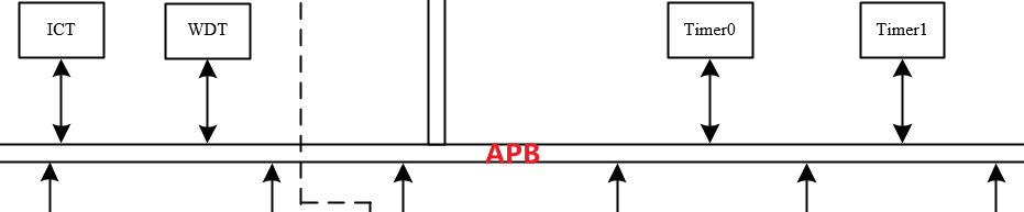
1.3.5、 Remaining components
In the lower left corner are the system controller and some analog components :
- System Controller: System controller
- POR:Power On Reset, Power on reset ( simulation IP)
- OSC:Oscillator, Crystal oscillator
- PLL:Phase Locked Loop, PLL
- VBG: Power management
- VR:Voltage Regulater, Voltage regulator
As mentioned above IO Small module , And the simulation components introduced in this section , We generally call it IP.
1.4、SoC - Bus BUS
Introduce the above IP Lines for interconnection , We call it bus . What we use here is AMBA 2.0 Bus , Include AHB、APB Two parts .
1.5、 Other modules
1.5.1、MemBist
MemBist Mainly aimed at Memory, Such as SRAM. In the manufacturing process , There may be defects , When the chip comes back , We are going to do some manufacturing tests !MemBist Is to conduct built-in self-test !
This built-in self-test is different from others IP Peripheral tests are different , other IP Peripheral tests usually pass GPIO Irrigation stimulation , Then the incentives after these logics are passed through others GPIO extraction , Then compare Partner. The built-in self-test is my test , Yes SRAM The test of does not need to pass the external pin , stay SRAM The exterior will be covered with Bist Logic , Then it is equivalent to triggering an enabling signal internally , Then it can go SRAM Fill various incentives , Then output the excitation after logic , You can complete such a built-in self-test . This is it. MemBist The function of .
1.5.1、Spare Cells
Spare Cells Mainly on the top , Used for post chip , I suddenly found that there was BUG, At this time, we should make a call ECO(Engineering Change Order, The process of manually modifying an integrated circuit ) Things that are , This time may involve some cell Replacement , If it has been released before Spare Cells Words , You can use it directly Spare Cells, There is no need to add again cell. If you add cells, May lead to the whole Die Can't fit ! So we reserved some for us in advance ECO To prepare the Spare Cells, Take up the area there , In this case , Whole FloorPlan No need to move !Cell Put it there , Try to influence our final FloorPlan.
1.5.1、IO MUX
Pin reuse , analogy STM32.
1.6、SoC IP
Two 、SoC Architecture diagram : sketch SoC Functions and application scenarios
- The chip is a SoC chip , The main functions are wireless communication and data storage function , The main application scenarios are Data cameras My memory card .
- wireless communication The function is through APB On the bus SPI The interface is connected with a WIFI chip , Realize the functions of wireless communication and data transmission .
- data storage The main function is NandFlash controller , Realize the storage function . But the chip uses an alternative , Used SD-Host Interface , external SD Card How to store data .
- The typical application scenario is : When taking pictures with a digital camera , Pass the photo through SD-Memory Controller interface , Put in SRAM The staging , Finally through SD Host Interface , Store photos in an external SD memory In the card , And then the cell phone /PC End user , Can be connected to WiFi On , By mobile phone /PC download SD Card Video stored in to mobile phone /PC.
- This application is used by reporters 、 shutterbug , Digital camera enthusiasts have application needs . When the pictures in the digital camera are downloaded to the mobile phone , You can use the mobile network , Upload to social media ; Live reporter , You can send photos to TV stations in time 、 The media provide timely photo materials .
- With the development of smart phones , Especially the development of HD cameras , The application scenario of this wireless memory chip scheme is shrinking .
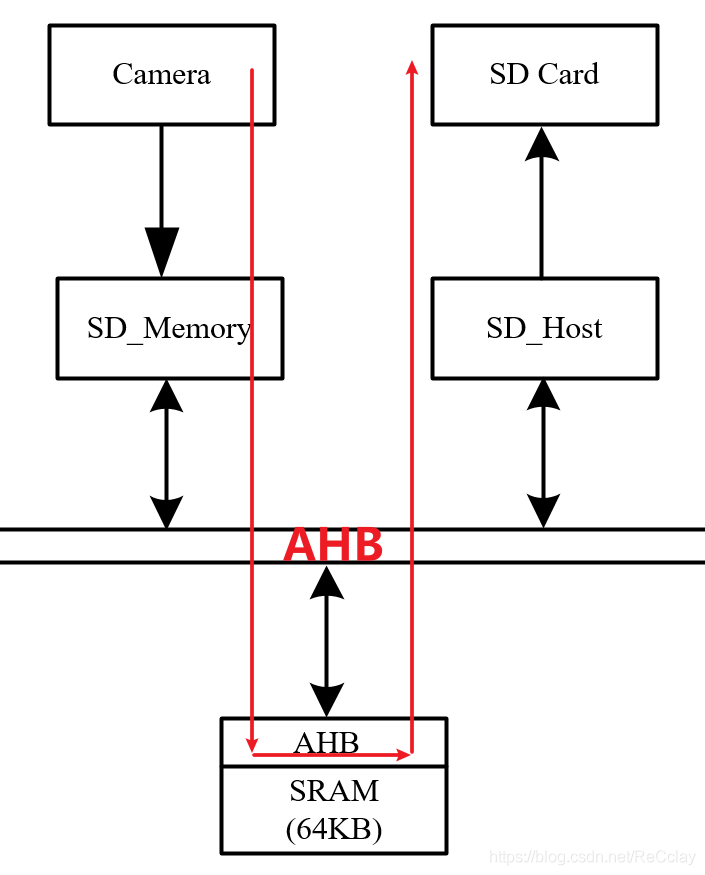
2.1、 data storage Data flow
data storage Functional Data flow To schematic diagram ( With DMA Move SRAM Take the data ): The data flow follows the arrow , In turn, is : red -> green -> blue .( The position of the label in the figure below is the starting position of the color )
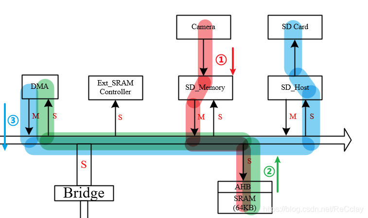
ask : Why not just from Camera -> SD Card? Here's the picture :
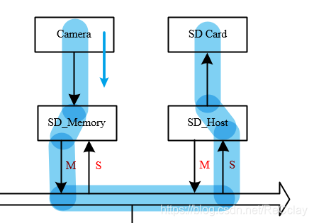
answer : Data path is accessible , however Camera The rate of sending data is the same as SD Card The rate at which data is stored , These two are not necessarily the same , This may lead to data errors . Store data SRAM, It's equivalent to a buffer The role of ! So after I save the data , Yes, save to SD Card Or through WiFi Wireless transmission , Both can pass CPU Flexible control !
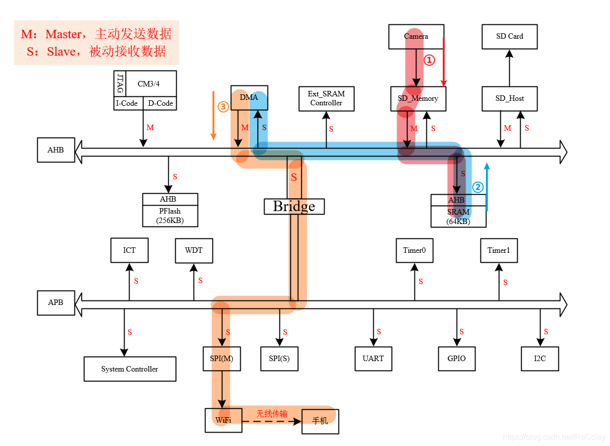
2.2、 Wireless transmission Data flow
Wireless transmission Functional Data flow To schematic diagram ( With DMA Move SRAM Take the data ): The data flow follows the arrow , In turn, is : red -> blue -> Brown .( The position of the label in the figure below is the starting position of the color )
2.3、 About Master and Slave
- CPU It's usually a Master, Originator of data ;
- The storage system (PFlash、SRAM) It's a Slave, Passively receive orders from others , To read the data of which address ;
- Two AHB High speed peripherals :SD_Memeory and SD_Host. both Master mouth , And then there is Slave mouth .SD_Memory When the module works , The data is through Master Port for transmission ,Slave Mouth refers more to CPU Configure it (IP It can work in many modes , The control signal can pass Slave Port to configure it );SD_Host The same applies to modules .
- Slow peripherals :SPI/UART/GPIO/I2C/Timer/WDT/ICT etc. , All are Slave mouth , yes CPU To tell them what data to send out (CPU Configure it ).
3、 ... and 、SoC Architecture diagram :IP Bus address mapping
Base address :Base Address
offset :Offset Address
notes :
Base address + offsetAnalogicalArea code + number. low 16 Bit is the offset address , high 16 Bit is the base address .
Every visit is based on the address space , Therefore, each system will be divided , Divide into an address space .
The peripheral addresses are shown in the following table :
| Block Name | Space SIze | Start Addr | End Addr |
|---|---|---|---|
| PFlash | 256K | 0x0000 0000 | 0x0003 FFFF |
| PFlash reg | 8K | 0x0006 0000 | 0x0006 1FFF |
| ext SRAM(nor) reg | 8K | 0x0007 0000 | 0x0007 1FFF |
| DMA | 8K | 0x0008 0000 | 0x0008 1FFF |
| SD Memory | 8K | 0x000A 0000 | 0x000A 1FFF |
| SD Host | 8K | 0x000C 0000 | 0x000C 1FFF |
| Timer0, Timer1 | 8K | 0x0020 0000 | 0x0020 1FFF |
| SPI-m | 8K | 0x0021 0000 | 0x0021 1FFF |
| ext SRAM(nor) | 128M | 0x8000 0000 | 0x87FF FFFF |
| SPI-s | 8K | 0x0022 0000 | 0x0022 1FFF |
| UART | 8K | 0x0023 0000 | 0x0023 1FFF |
| GPIO | 8K | 0x0024 0000 | 0x0024 1FFF |
| I2C | 8K | 0x0026 0000 | 0x0026 1FFF |
| ICT | 8K | 0x0028 0000 | 0x0028 1FFF |
| WDT | 8K | 0x0029 0000 | 0x0029 1FFF |
| system controller | 8K | 0x002A 0000 | 0x002A 1FFF |
| SRAM | 64K | 0x0040 0000 | 0x0040 FFFF |
When software engineers write modules , Usually only focus on the offset address !
- Generally, an address space can store 8bit data , Therefore, the above units are
KB
Four 、SoC Architecture diagram :Pin-MUX & PAD
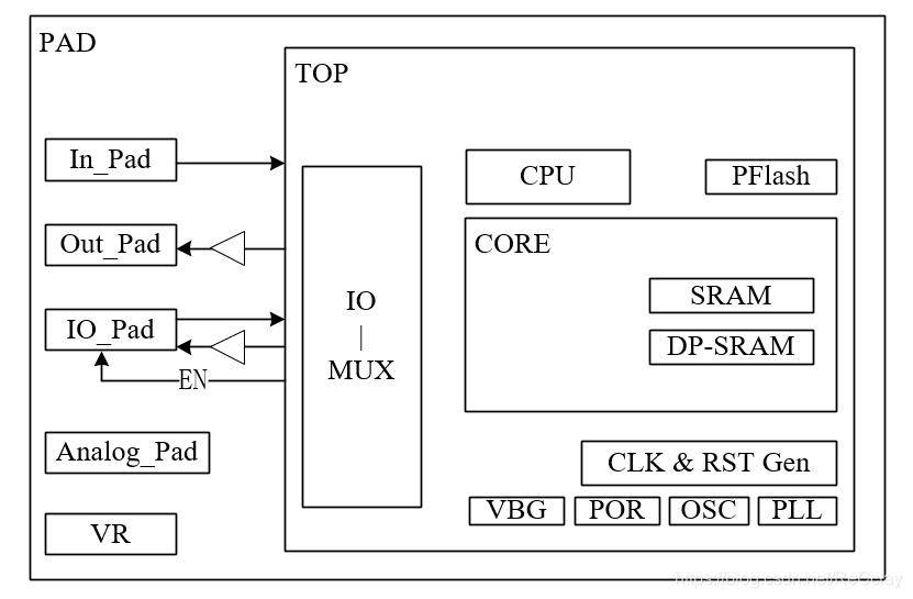
- PAD: An interface between chip and external communication
- PIN-MUX: Mainly used to reduce PAD number , Why reduce PAD?
- ①、PAD It's big in itself ,PAD Too much , It takes up a lot of side length , Cause Planning Die can't let go .【 Enough margin shall be reserved for the peripheral side length of the chip 】
- ②、PAD Itself is a simulator ,PAD Too much , Will increase power consumption !【 Overall power consumption will also benefit 】
- The above figure shows three Numbers PAD, From top to bottom are :Input Only、Output Only、Bidirection Three . Engineering is usually Bidirection , Direct control when using EN The signal , Make it input or output !
- simulation PAD: Such as LVDS;
- VR( Voltage regulator ) PAD
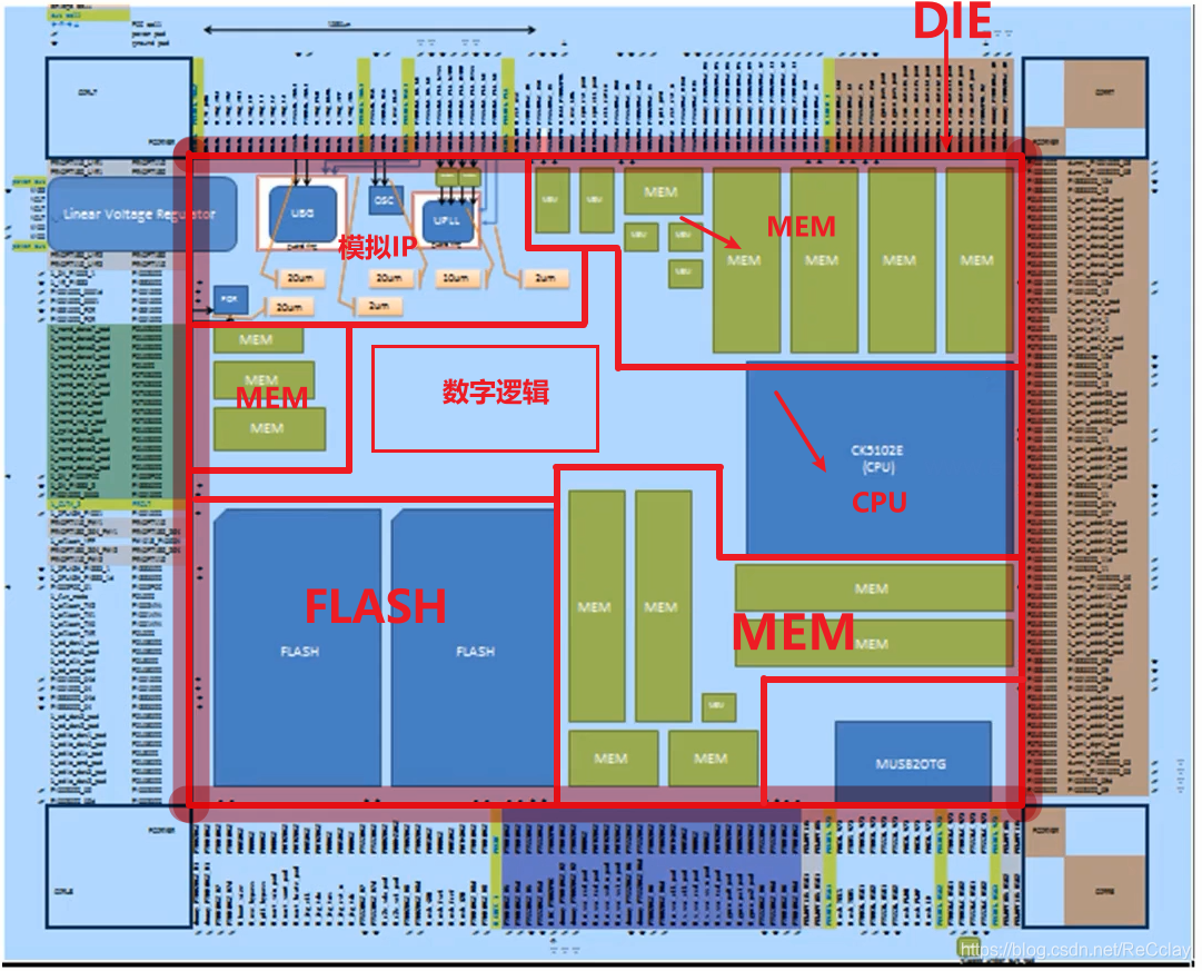
5、 ... and 、SoC Architecture diagram : Layout Floorplan
notes : Layout Floorplan The layout can be compared PCB Of Layout !
Floorplan You can see all Cell( digital circuit ) And each IP( Analog circuit ).
- simulation IP (MEM/FLASH) Put it close DIE Of Corner On , Improve space utilization
- DIE Of Inside Can put Digital logic
This placement principle is for Improve the utilization of the whole space !MEM This simulation IP, It can be considered as a hard core , If it is placed in the middle , Then the surrounding winding will be very troublesome . If it's numbers , That is each discrete Cell, The wiring is easy , High space utilization !
6、 ... and 、SoC Architecture diagram : Territory layout - GDSII
notes : Territory layout Analogical PCB Of wiring !
The following layout layout in , The purple part in the middle is the corresponding Floorplan The digital logic part marked in , Close to Die What we need is simulation IP!
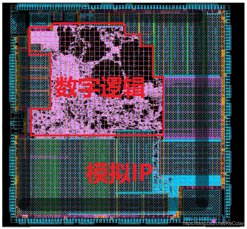
- Level of workmanship :110nm e-flash
- DIE size :3mm x 4mm = 12 mm^2
- wafer wafer size :8 Inch , Can generate 3600 slice DIE(3mm x 4mm),1 individual wafer The manufacturing cost of 1000 dollar .
- Yield (yield)【wafer How many of them DIE Is available 】:>95%( adopt ATE To screen for useless DIE)
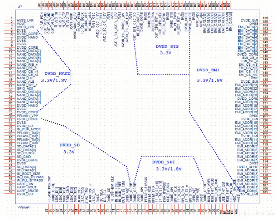
6、 ... and 、SoC Architecture diagram :Pin & Supply voltage
The following figure is the schematic diagram of the periphery , From it, we can see the pin distribution and voltage domain division .
- The division of voltage domain is usually completed by architects , Front end personnel can't touch this thing !
- The voltage domain can usually be divided into : Digital voltage domain (CORE、IO)、 Analog voltage domain ( Different simulations IP, Different voltages )
7、 ... and 、 Digital system design node (SoC Design Node)
The birth of chips , The whole process from early stage to late stage :
- ①、 Conduct market research , Is there any market demand , Does it have good commercial value , Making chips costs money ,1 individual wafer1w dollar , And buy some IP It costs money to wait ! Can you make money after making it , Does anyone pay for it , This is very important !
- ②、 According to market demand , The algorithm team depends on the function to be realized , Make an algorithm model , Algorithms can be implemented ( The simulation is successful ), It can meet the market demand , Then go to the next step .
- ③、 Design the implementation architecture of the chip , Include : Hardware and software partition ( Which parts are implemented by software , Which parts are implemented in hardware )、 How many modules are divided in hardware , Write architecture documents (AS,Architecture Specification), The architecture is also divided into many levels , Such as system level , Circuit level, etc . Next, write a design document (DS,Design Specification)
- ④、 To write RTL Code , Perform functional verification (EDA Simulation verification 、FPGA Prototype verification ) And code review
- ⑤、 Through comprehensive tools , Convert it to Netlist, the RTL Code mapping (MAP) Form a gate level net list (STD CELL), Conduct formal verification at the same time (RTL Logical functions and Netlist Logical function comparison of , See if the comprehensive tools put RTL Some functions are optimized ), Timing verification ( Realization Netlist after ,timing setup Can you meet )
- ⑥、 Next, physical implementation ,GDSII It is also a net list , It's just a net list containing device location information .Netlist Just logical information . Then conduct some post simulation and sign in Review .
- ⑦、 Casting , stay wafer Generate our chip on . Is there any problem in the production process , adopt ATE test ,ATE The test of partner It's done in front RTL At the time of the DFx It's done ,Membist,Scan scanning , They are all designed in the early stage , After the chip comes back , Will start these circuits , Conduct ATE test ! Test the chip itself , Is there a manufacturing function problem !
- ⑧、 Finally, the application test , Functional testing . Put on the market .
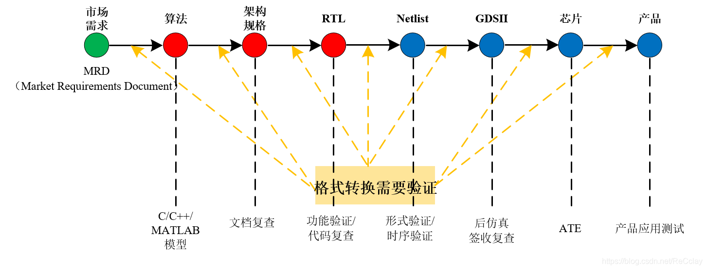
As you can see from the picture above
- ①、 The implementation of the chip requires a lot of teams , Many links , Step by step .
- ②、 The deliverables of each link ( Delivery criteria ) It is changing. , Each step requires different methods of verification . do IC verification , Mainly on RTL Functional verification of , Make clear the position of the work in the whole design process !
Basic skills 、 Expertise
Reference resources
边栏推荐
猜你喜欢
CVPR 2022 | 常见3D损坏和数据增强
Unity编辑器扩展 UI控件篇
![[quick start of Digital IC Verification] 9. Finite state machine (FSM) necessary for Verilog RTL design](/img/32/a156293f145417eeae8d93c539ca55.png)
[quick start of Digital IC Verification] 9. Finite state machine (FSM) necessary for Verilog RTL design
Leetcode brush question: binary tree 14 (sum of left leaves)
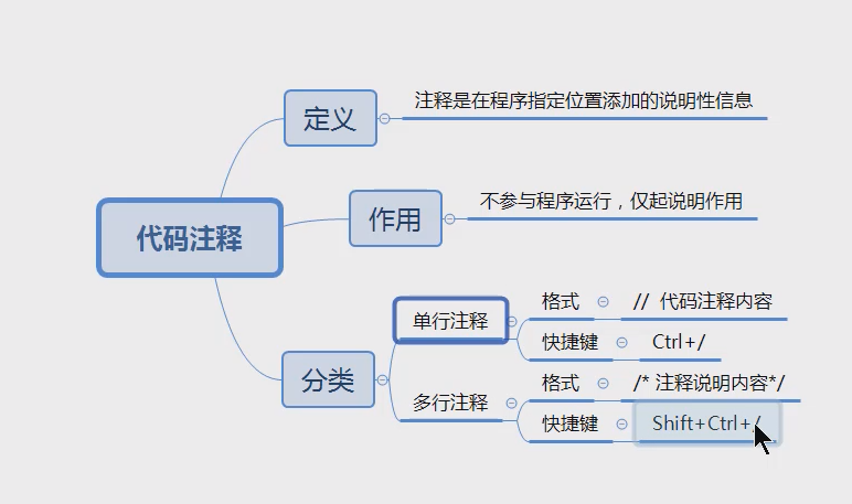
【愚公系列】2022年7月 Go教学课程 004-Go代码注释
![信息学奥赛一本通 1339:【例3-4】求后序遍历 | 洛谷 P1827 [USACO3.4] 美国血统 American Heritage](/img/f0/0f985425bd61d9852af0b5fd7307ee.png)
信息学奥赛一本通 1339:【例3-4】求后序遍历 | 洛谷 P1827 [USACO3.4] 美国血统 American Heritage
基础篇——配置文件解析
Applet event binding
Enter the parallel world
A way to calculate LNX
随机推荐
19 mongoose modularization
USACO3.4 “破锣摇滚”乐队 Raucous Rockers - DP
港股将迎“最牛十元店“,名创优品能借IPO突围?
model方法
2022北京眼睛健康用品展,护眼产品展,中国眼博会11月举办
National Eye Care Education Conference, 2022 the Fourth Beijing International Youth eye health industry exhibition
Ros2 topic [01]: installing ros2 on win10
y57.第三章 Kubernetes从入门到精通 -- 业务镜像版本升级及回滚(三十)
Scala basics [HelloWorld code parsing, variables and identifiers]
【数字IC验证快速入门】1、浅谈数字IC验证,了解专栏内容,明确学习目标
[quick start of Digital IC Verification] 3. Introduction to the whole process of Digital IC Design
ByteDance dev better technology salon was successfully held, and we joined hands with Huatai to share our experience in improving the efficiency of web research and development
A way to calculate LNX
Leetcode brush questions: binary tree 18 (largest binary tree)
Codeforces Round #804 (Div. 2) - A, B, C
Unity编辑器扩展 UI控件篇
Informatics Olympiad 1340: [example 3-5] extended binary tree
怎么挑选好的外盘平台,安全正规的?
Classic implementation of the basic method of intelligent home of Internet of things
C language OJ gets PE, OJ of ACM introduction~