当前位置:网站首页>Write CPU yourself -- Chapter 9 -- learning notes
Write CPU yourself -- Chapter 9 -- learning notes
2022-07-07 07:35:00 【code_ master2020】
Chapter will realize MIPS32 Load and store instructions defined in the instruction set architecture , A two-step : First, divide ll、sc General load storage instructions outside the instructions , Secondly, it implements special loading and storage instructions ll、sc.
9.1 Description of load storage instruction
MIPS32 The load and store instructions defined in the instruction set architecture share 14 strip , as follows :
--8 Load instructions :lb、lbu、lh、lhu、ll、lw、lwl、lwr
--6 Storage instructions :sb、sc、sh、sw、swl、swr
9.1.1 Load instruction lb、lbu、lh、lhu、lw explain
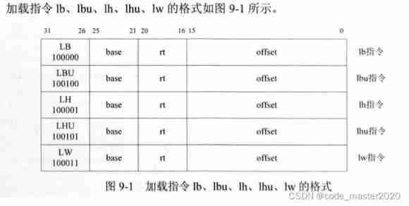 this 5 Loading instructions can be based on 26~31bit The instruction code of , in addition , The... Of the loading instruction 0~15bit yes offset、 The first 21~15bit yes base, The calculation method of loading address is as follows , First the 16 Bit offset Symbols extended to 32 position , And then with the address base Add the values of the general-purpose register , You can get the loading address .
Load address = signed_extended(offset) + GPR[base]
9.1.2 Store instructions sb、sh、sw explain

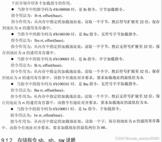
From the picture 9-2 You know , this 3 Storage instructions can be based on 26~31bit The instruction code of , in addition , The... Of the storage instruction 0~15bit yes offset、 The first 21~25bit yes base, The calculation method of storage address is as follows , First the 16 Bit offset Symbols extended to 32 position , And then with the address base Add the values of the general-purpose register , You can get the storage address .
Storage address = signed_extended(offset) + GPR[base]
9.1.3 Load storage instruction usage example
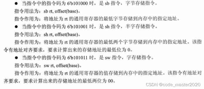
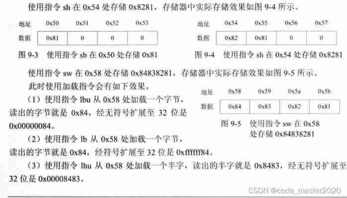
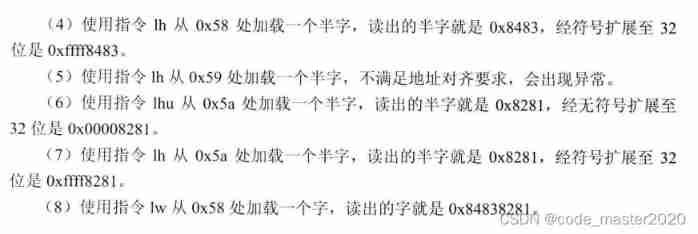
OPenMIPS The processor is addressed by bytes , And it is the big end mode , In this mode , The high bit of data is stored in the low address of memory , The low order of the data is stored in the high address of the memory . such as : Use instruction sb stay 0x50 Store 0x81, The actual storage effect of the memory is shown in the figure .
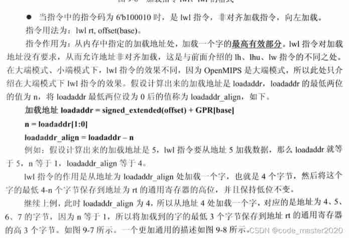
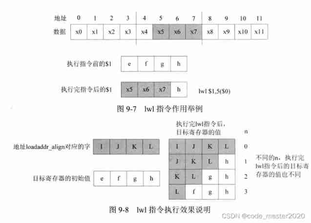
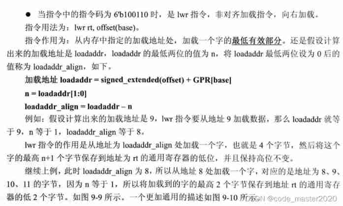
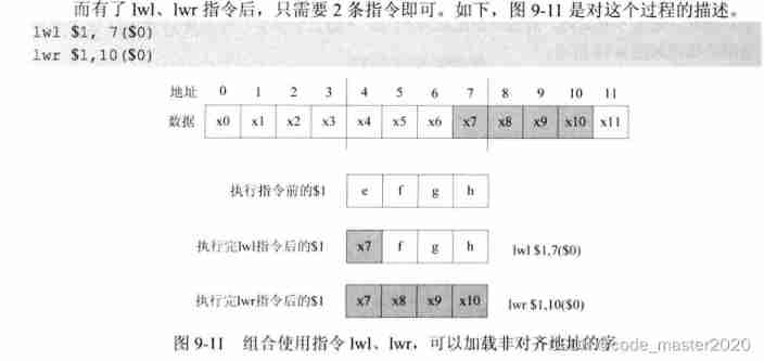
9.1.4 Load instruction lwl、lwr explain

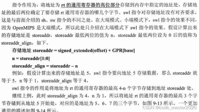
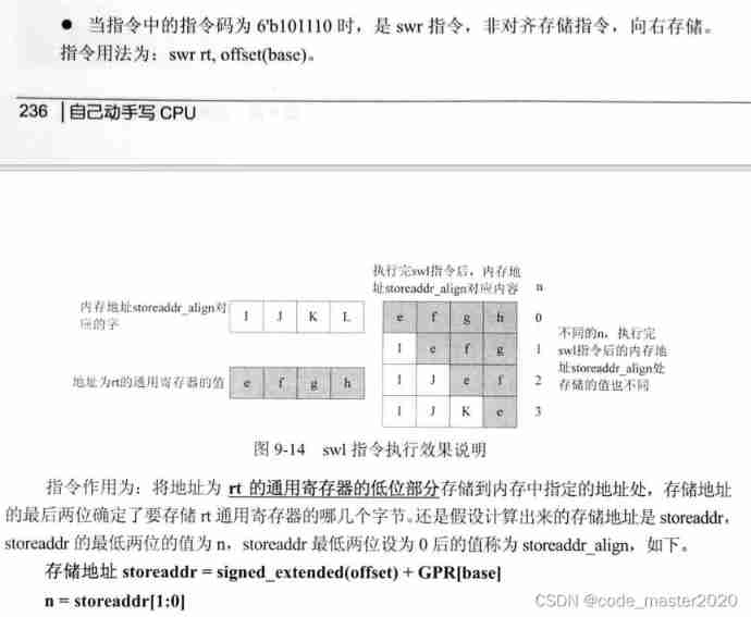
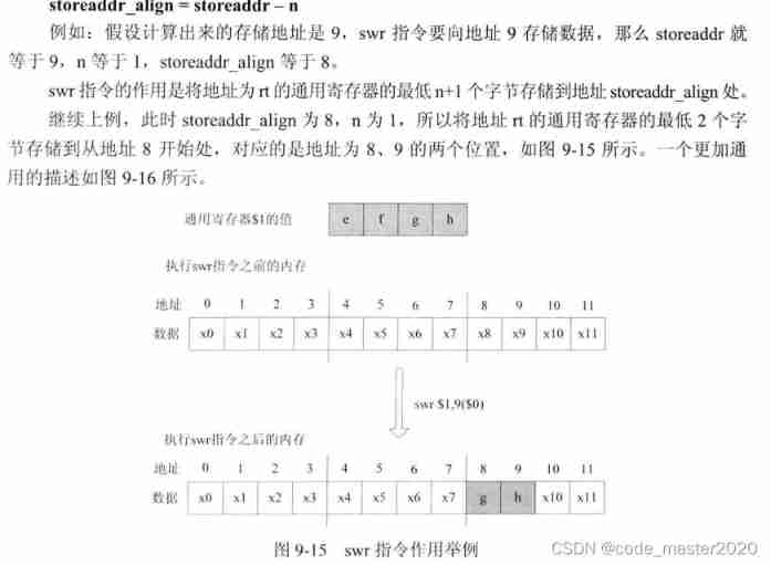
9.1.5 Store instructions swl、swr explain 

2 Implementation idea of loading and storing instructions
Section introduces in addition to ll、sc The implementation idea of loading and storing instructions outside ,ll、sc The implementation idea of the instruction will be 9.7 Section special introduction
1. Loading instruction implementation ideas
The loading instruction is decoded in the decoding stage , Get the operation type alusel_o、aluop_o, And the destination register information to be written . This information is passed to the execution stage , Then it is transferred to the deposit access stage , The storage access stage is based on this information , Set to data memory RAM Access signal for . from RAM The data read back needs to be loaded according to the type of instruction 、 Load address for alignment adjustment , The adjusted result is the data of the destination register to be written finally .
2. Memory instruction implementation ideas
The stored instructions are decoded in the decoding stage , Get the operation type alusel_o、aluop_o, And the data to be stored , This information is passed to the execution stage , Then it is transferred to the deposit access stage , The storage access stage is based on this information , Set to data memory RAM Access signal for , Write data to RAM.
Here's the thing to watch out for : This chapter assumes that the external data memory can be completed in one clock cycle RAM Read and write operations , Implement the practice version in the following chapters OpenMIPS The processor will consider complex situations .
9.2.1 Modification of data flow diagram
In order to achieve division ll、sc Load storage instructions other than , Modify the data flow diagram . Mainly in the memory access stage, the data memory is added RAM The interview of , meanwhile , Because the data to be written to the destination register may be the result of the execution stage , It may also be from the data memory during the memory access stage RAM Load the obtained data , Therefore, a multiplexer is added in the memory access stage , Make a selection .
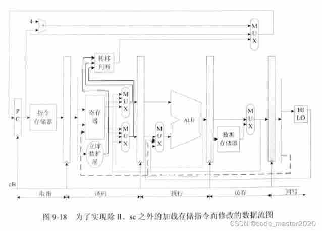
9.2.2 Modification of system structure
In order to achieve division ll、sc Load storage instructions other than , The system structure needs to be modified , Add interfaces of some modules .
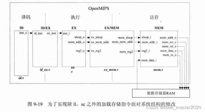
The main changes are as follows .
(1) Decoding stage ID The module adds an output signal inst_o, Its value is the instruction in the decoding stage , This signal is passed to the execution phase , In the implementation phase EX The module will use the value of this signal to calculate the load 、 Storage address mem_addr_o.
(2) Implementation phase EX Module will be operator type aluop_o、 Load storage address mem_addr_o、 The second operand read reg2_o Etc , adopt EX/MEM The module is passed to the memory access stage MEM modular .
(3) In the deposit access stage MEM Modules are loaded according to 、 Type of stored instruction , Make sure that the data storage RAM Access information for , adopt mem_ce_o Interface sends data memory enable signal ,mem_addr_o The interface sends out the access address ,mem_we_o The interface indicates whether to load or store 、mem_sel_o The interface sends a byte selection signal , If it is a storage instruction , Then it passes mem_data_o The interface outputs the data to be stored , If it's a load instruction , So from mem_data_i Interface to get the read data , then MEM The module depends on the specific type of loading instruction 、 Load address , Align and adjust the acquired data , Finally get the data to be written to the destination register .
9.3 modify OpenMIPS To load storage instructions
9.3.1 Modify the decoding stage
1. modify ID modular
ID Add interfaces to the module inst_o. stay ID The module also needs to add the analysis of loading and storage instructions , The instruction codes of these instructions are different , So you can directly determine which instruction is based on the instruction code
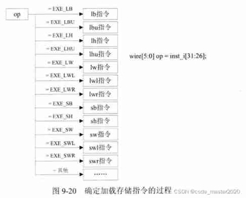
The main task of decoding is to determine the destination register to be written 、 Registers to be read and operations to be performed . The following describes the decoding process of several representative instructions .
(1)lb Instructions
-- Destination register to write : Load instruction lb The loading result needs to be sucked into the destination register , So set wreg_o by WriteEnable, At the same time, we can see , The destination register address to be written is the... In the instruction 16~20bit, So set wd_o by inst[20:16].
-- Register to read : The address used to calculate the loading target address is base The register value of , So set reg1_read_o by 1, Said by RegFile Read port of the module 1 Read the value of the register , Default read register address reg1_addr_o It is the first of the instructions 21~25bit, It is lb Directive base. So the output of the final decoding stage reg1_o The address is base The value of the register for .
-- The operation to be performed : Set up alusel_o by EXE_RES_LOAD_STORE, Indicates that the operation type is load storage , Set up aluop_o by EXE_LB_OP, Indicates that the operator type is byte loading lb.
lbu、lh、lhu、lw Command and lb The decoding process of instructions is similar , knowledge aluop_o The value is different. .
(2)lwl Instructions
-- Destination register to write : Load instruction lwl The loading result needs to be sucked into the destination register , So set wreg_o by WriteEnable, At the same time, we can see , The destination register address to be written is the... In the instruction 16~20bit, So set wd_o by inst[20:16].
-- Register to read : The address used to calculate the loading target address is base The register value of , So set reg1_read_o by 1, Said by RegFile Read port of the module 1 Read the value of the register , Default read register address reg1_addr_o It is the first of the instructions 21~25bit, It is lwl Directive base. So the output of the final decoding stage reg1_o The address is base The value of the register for . Besides , because lwl The instruction only partially modifies the destination register , therefore , Set up reg2_read_o Also for the 1 Said by RegFile Read port of the module 2 Read the value of the register , Default read register address reg2_addr_o It is the first of the instructions 16~20bit, It is lwl Directive rt. So the output of the final decoding stage reg2_o The address is rt The value of the register for .
-- The operation to be performed : Set up alusel_o by EXE_RES_LOAD_STORE, Indicates that the operation type is load storage , Set up aluop_o by EXE_LWL_OP, Indicates that the operator type is byte loading lwl.
lwr Command and lwl The decoding process of instructions is similar , It's just aluop_o The value is different. .
(3)sb Instructions
-- Destination register to write : Load instruction sb The loading result needs to be sucked into the destination register , So set wreg_o by WriteEnable, At the same time, we can see , The destination register address to be written is the... In the instruction 16~20bit, So set wd_o by inst[20:16].
-- Register to read : The address used to calculate the loading target address is base The register value of , So set reg1_read_o by 1, Said by RegFile Read port of the module 1 Read the value of the register , Default read register address reg1_addr_o It is the first of the instructions 21~25bit, It is sb Directive base. So the output of the final decoding stage reg1_o The address is base The value of the register for . The value to be stored is the value of the general register , therefore , Set up reg2_read_o Also for the 1 Said by RegFile Read port of the module 2 Read the value of the register , Default read register address reg2_addr_o It is the first of the instructions 16~20bit, It is sb Directive rt. So the output of the final decoding stage reg2_o The address is rt The value of the register for .
-- The operation to be performed : Set up alusel_o by EXE_RES_LOAD_STORE, Indicates that the operation type is load storage , Set up aluop_o by EXE_SB_OP, Indicates that the operator type is byte loading sb.
sh、sw、swr、swl Command and sb The decoding process of instructions is similar , It's just aluop_o The value is different. .
2. modify ID/EX modular
ID/EX The module needs to add some interfaces , Is used to ID The newly added output signal of the module inst_o Passed to the execution phase EX modular .

9.3.2 Modify the execution phase
1. modify EX modular
In the implementation phase EX The module will calculate the destination address of the load storage , Refer to the figure 9-19 You know ,EX The module will add some interfaces , As shown in the table 9-3 Shown .
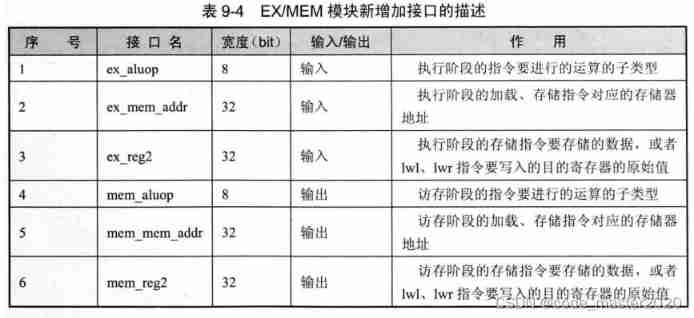
2. modify EX/MEM modular
Refer to the figure 9-19 You know ,EX/MEM The module will add some interfaces , be used for EX The output added by the module is transferred to the memory access stage
9.3.3 Modify the storage access stage
The storage access stage is mainly to modify MEM modular , Refer to the figure 9-19 You know , You need to add a pair of data storage for it RAM Access interface .
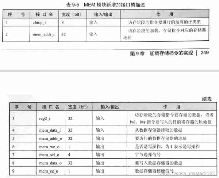
Here's the answer to mem_sel_o Make further explanation , Split loading 、 The two storage operations are described separately .
(1) For load operation ,MIPS32 The load instruction defined in the instruction set architecture can load bytes 、 Half word 、 word , But the width of the data bus is 32 position , Occupy 4 Bytes . If the load byte instruction is executed lb、lbu, Then you need to know what is input through the data bus 4 In bytes , Which byte is the data to be read : If the load halfword instruction is executed lh、lhu, Then you need to know which half word is the data to be read ,mem_sel_o The function of is to point out which part is valid data .mem_sel_o The width is 4, Corresponding to... Of data bus respectively 4 Bytes , such as : Use the load instruction lb Read data memory address 0x1 Bytes out , Then you can set mem_sel_o by 4'b0100, It means , You want the external memory to output data , Address 0x1 Place the bytes at 32 The next highest byte of the bit data bus , That is the first. 16~23bit The location of , When data is sent to the processor , The processor takes out the first 16~23bit Corresponding bytes , As data memory address 0x1 Place the value of the .
(2) For storage operations ,MIPS32 The storage instructions defined in the instruction set architecture can store bytes 、 Half word 、 word , But the width of the data bus is 32 position , Occupy 4 Bytes , If the byte storage instruction is executed sb、 Half word storage instructions sh, Then the external data memory should know that it has been transferred by the data bus 4 In bytes , Which byte 、 Which half word is the data to be stored ,mem_sel_o The function is to point out which part is the valid data to be stored . such as : Use storage instructions sh To address 0x2 Store 0x8281, Then you can set mem_data_o by 0x82818281、 Set up mem_sel_o by 4'b0011, In this way, the external memory knows that the data to be stored is 0x82818281 The lowest two bytes of , It is 0x8281.
The following explains the memory access process of several typical instructions
(1) Because you need to access the data storage , So set mem_ce_o by ChipEnable
(2) Because it is a loading operation , So set mem_we_o by WriteDisable
(3) Give the address of the data memory to be accessed mem_addr_o, Its value is the address calculated at the execution stage mem_data_i.
(4) basis mem_addr_i The last two of , determine mem_sel_o Value , And according to this, input from the data memory mem_data_i Get the bytes to read , Expand the symbols . such as : If mem_addr_i The last two of you are 01, Then set mem_sel_o by 4'b0100, Indicates that you want to output the data given by the memory 16~23bit Is the bytes to be read , That is to say mem_data_i[23:16], Sign the highest bit , Get the final result wdata_o, As the data to be written to the target register .
2.lwl Instruction memory access process
(1) Because you need to access the data storage , So set mem_ce_o by ChipEnable
(2) Because it is a loading operation , So set mem_we_o by WriteDisable
(3) Give the address of the data memory to be accessed mem_addr_o, Its value is the address calculated at the execution stage mem_data_i., But the last two digits should be set to 0, because lwl Instructions should start from RAM Read a word in , So you need to align the address , Simultaneous setting mem_sel_0 by 4'b1111.
(4) basis mem_addr_i The last two of , Data to be read from the data memory mem_data_i And the original value of the destination register reg2_i Are combined , Get the value to be finally written to the destination register wdata_o,
3.sb Instruction memory access process
(1) Because you need to access the data storage , So set mem_ce_o by ChipEnable.
(2) Because it is a storage operation , So set mem_we_o by WriteEnable.
(3) Give the address of the data memory to be accessed mem_addr_o, Its value is the address calculated at the execution stage mem_addr_i.
(4)sb The data to be written by the instruction is the lowest byte of the register , Copy this byte to mem_data_o The rest of , Then according to mem_data_i The last two of , determine mem_sel_o Value .
4.swl Instruction memory access process .
9.4 Minimum modification SOPC
To verify whether the loading and storage instructions added in the previous section are implemented correctly , The minimum design in Chapter 4 needs to be modified SOPC, Add data storage to it RAM.
9.4.1 Add data storage
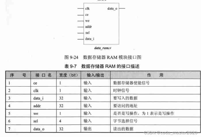
9.6 Link load instructions ll、 Conditional storage instruction sc explain
ll、sc Instruction is MIPS32 Instructions MIPS32 The special loading and storage instructions in the instruction set architecture , Used to implement semaphore mechanism . In a multithreaded system , need RMW(Read-Mpdify-Write) The sequence of operations guarantees the exclusivity of a resource ,RMW The meaning of operation sequence is , Read data from an address in memory , Read hungry data after modification , Then save it back to the original memory address , There should be no interference in this process , Therefore, it is necessary to establish a critical region (Critical Region), Operations performed in critical regions are often referred to as atomic operations , Atomic operations cannot be disturbed . The way the operating system establishes adjacent areas is usually the semaphore mechanism , as follows .
wait(semaphore);
Atomic manipulation
signal(semaphore);
semaphore It's a semaphore , by 1 Indicates that the semaphore is in use , by 0 Indicates that the semaphore is idle . Before atomic operations , Use wait Function query semaphore Value , If 1, Is waiting for , otherwise , Set it to 1, Start atomic operation . After operation ,signal Function will semaphore Set as 0, In this way, other threads can perform atomic operations .
It should be noted that ,wait The execution of a function is also an atomic operation , It's a kind of “ Detection before setting ” The operation of (tesr-and -set operation), This operation generally does not want to be interrupted by external devices , And don't want to be interrupted by other threads , Many processors have special instructions for solid " Detection before setting " operation . This is also a semaphore mechanism .
MIPS32 The architecture adopts a special way to realize the semaphore mechanism , For atomic operations ,MIPS32 Architecture does not guarantee that it must be atomic , That is, it allows detection and setting to run without atomicity guarantee , But only when it is really the operation of atoms can we make “ Set up ” take effect .MIPS32 The architecture uses link loading instructions ll、 Conditional storage instruction sc To implement this semaphore mechanism .
ll Instructions are the same as general load instructions , Load a word from memory , however , It's a little different ,ll The instruction will also link a link status bit inside the processor LLbit Set as 1, Indicates that a link loading operation has occurred , And save the linked address to a special register LLAddr in .
ll After the instruction is executed , Will carry out certain operations ( Such as : The modified data is loaded ), And then execute sc Instructions , This can be thought of as a RMW Sequence . There are two cases, dry meat RMW Sequence , After being disturbed , The processor will set the link status bit LLbit by 0
-- stay ll、sv An exception occurred between instructions , To enter the exception handling routine , Or thread switching occurs , boil RMW Xu Lei was disturbed .
-- In multiprocessor systems , the other one CPU Rewrite the RMW Memory space to be operated by the sequence .
about OpenMIPS for , Only the first one 1 In this case .
perform sc When the command , Will be right from ll The beginning of the command RMW Check the sequence , Judge whether it is disturbed , Reality is judgment LLbit whether wie1, If there is no interference ,LLbit Keep for 1, Then the operation is atomic ,sc Instructions will be directed to ll The instruction loads the address of the data for write back operation , And set the value of a general register to 1, It means success , On the contrary, no writeback operation is performed , And set the value of a general register to 0, It means failure .


9.7ll、sc Instruction implementation ideas
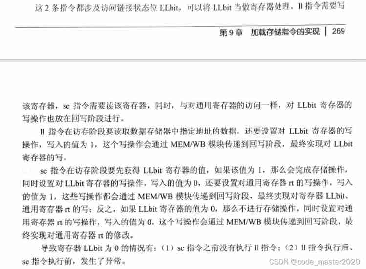
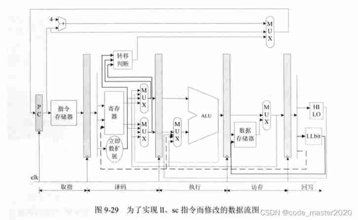
9.7.2 Modification of data flow diagram
9.7.3 Modification of system structure
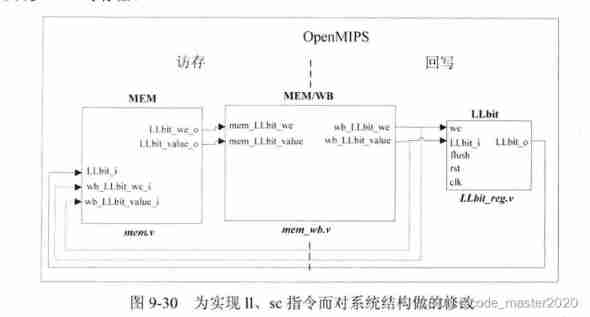
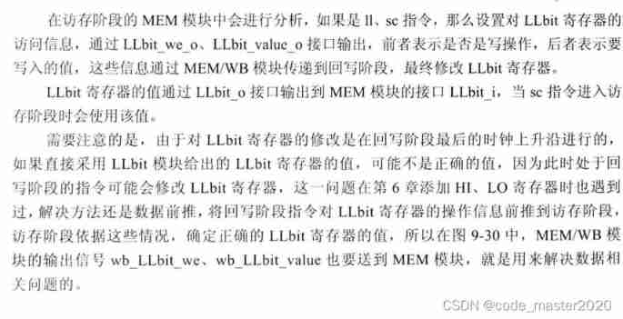
9.8 modify OpenMIPS In order to realize the ll、sc Instructions
9.8.2 Modify the decoding stage ID modular

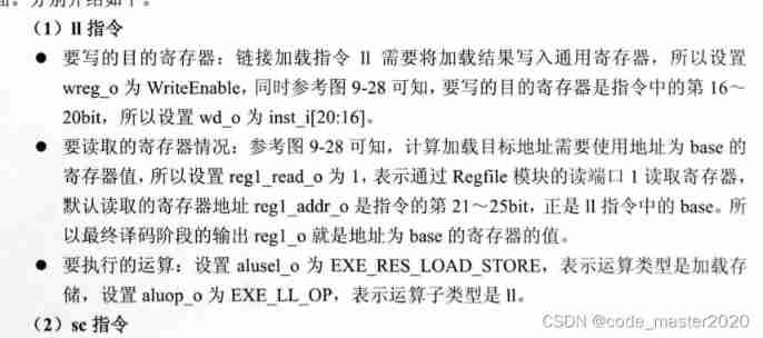
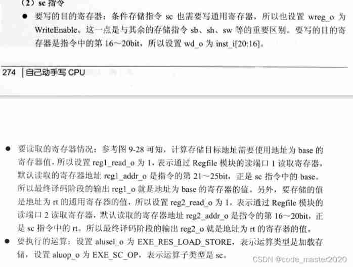
9.8.3 Modify the storage access stage
边栏推荐
- Deep learning Flower Book + machine learning watermelon book electronic version I found
- Leetcode sword finger offer brush questions - day 20
- Build personal website based on flask
- My ideal software tester development status
- Tencent's one-day life
- FullGC问题分析及解决办法总结
- Advanced level of C language (high level) pointer
- 弹性布局(二)
- Freeswitch dials extension number source code tracking
- Several important steps to light up the display
猜你喜欢
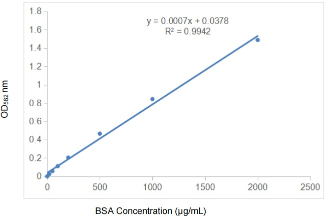
Fast quantitative, abbkine protein quantitative kit BCA method is coming!
![[2022 CISCN]初赛 web题目复现](/img/1c/4297379fccde28f76ebe04d085c5a4.png)
[2022 CISCN]初赛 web题目复现

Wechat applet full stack development practice Chapter 3 Introduction and use of APIs commonly used in wechat applet development -- 3.10 tabbar component (I) how to open and use the default tabbar comp
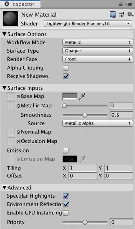
URP - shaders and materials - light shader lit
Outsourcing for four years, abandoned

外包干了三年,废了...
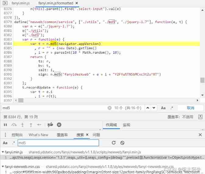
English translation is too difficult? I wrote two translation scripts with crawler in a rage
1089: highest order of factorial
Advanced practice of C language (high level) pointer
弹性布局(一)
随机推荐
Blue Bridge Cup Birthday candles (violence)
Differences between H5 architecture and native architecture
"Xiaodeng in operation and maintenance" meets the compliance requirements of gdpr
电商常规问题part1
Mutual conversion between InputStream, int, shot, long and byte arrays
計算機服務中缺失MySQL服務
1140_ SiCp learning notes_ Use Newton's method to solve the square root
PostgreSQL source code (59) analysis of transaction ID allocation and overflow judgment methods
Blue Bridge Cup Netizen age (violence)
Pass parent component to child component: props
基于Flask搭建个人网站
Outsourcing for four years, abandoned
【性能压测】如何做好性能压测?
Communication of components
按键精灵采集学习-矿药采集及跑图
PostgreSQL source code (60) transaction system summary
关于二进制无法精确表示小数
About some details of final, I have something to say - learn about final CSDN creation clock out from the memory model
Outsourcing for three years, abandoned
Model application of time series analysis - stock price prediction