当前位置:网站首页>[Digital IC hand tearing code] Verilog burr free clock switching circuit | topic | principle | design | simulation
[Digital IC hand tearing code] Verilog burr free clock switching circuit | topic | principle | design | simulation
2022-07-06 22:18:00 【myhhhhhhhh】
| Chip design verification community · Where chip lovers gather · Hardware related discussion community · Numbers verifier star |
|---|
| Four communities Jointly recommend ! near 500 piece Numbers IC Collection of excellent articles ! |
| 【 Numbers IC Collection of excellent articles 】 Learning route · Basic knowledge of · Bus · Scripting language · Chip job search ·EDA Tools · Low power design Verilog·STA· Design · verification ·FPGA· framework ·AMBA· Books |

Verilog Burr free clock switching circuit
One 、 Preface
This series aims to provide 100% Accurate numbers IC Design / Verify the title of the hand tearing code link , principle ,RTL Design ,Testbench And reference simulation waveform , The content of each article is checked by simulation . The quick navigation links are as follows :
1. Odd frequency division
2. Even frequency division
3. Semi integer batch
4. decimal / Fractional frequency division
5. Sequence detector
6. Mode three detector
7. Beverage machine
8. Asynchronous reset , Simultaneous release
9. Edge detection ( Rising edge , Falling edge , On both sides )
10. Full adder , Half adder
11. Gray code to binary
12. single bit Cross clock domain ( Two beats , Edge synchronization , Pulse synchronization )
13. Parity check
14. Pseudo random number generator [ Linear feedback shift register ]
15. Sync FIFO
16. Burr free clock switching circuit
Ought to say , The hand tearing code link is in the interview process Both important and simple A part of , Compared with software jobs , Numbers IC Hand tear code Fixed topic , Limited number , It belongs to a link that must be scored in the whole interview , Outside this series , I also recommend numbers IC Job seekers use “HdlBits” Code Training
Links are as follows
HDLBits — Verilog Practice
Two 、 subject
in order to SOC Low power consumption of the design , Division of multi clock domain Is one of the common means , There are two clocks ,A by 50Mhz,B by 100Mhz, please Design a burr free clock switching circuit , According to the control signal control, Output the required clock signal .
3、 ... and 、 principle
3.1 Clock switching with burrs
Want to switch the clock circuit , The easiest way is definitely to use a MUX,control As Control signals
control=1,clk_output = clk_50M,
control=0,clk_output =clk_100M,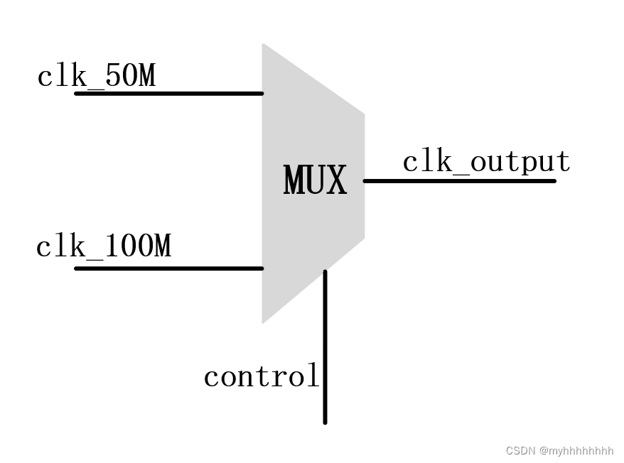
But there will be burrs in this practice , As shown in the figure , When control When the edge of signal conversion , If clk_50M And clk_100M The edge of is not aligned , There may be burrs , Affect clock quality 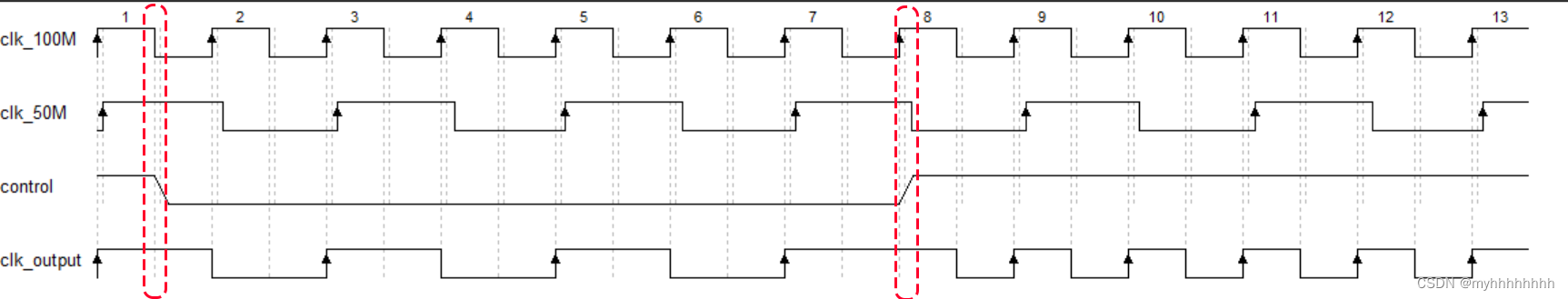
So we need to Burr free clock switching circuit With the help of the , Go to the next section
3.2 Burr free clock switching
First of all, we need to be clear about , Cause of burr
control The signal Asynchronous signal for at least one clock signal , Caused the appearance of burrs , If control,clk_50M, still clk_100M All are Ideal signal with fully synchronized edges word , Should be There will be no burrs .
therefore Methods to avoid burrs Naturally, the transition to “ Asynchronous signal synchronization ” This theory is above , How to synchronize ?
without doubt , Must be Need to shoot / Sampled by The way
Is the rising edge synchronized or the falling edge synchronized ?
Here is the rising edge beat or the falling edge beat, which is actually It varies with the circuit A question of , If we hope to finally Use and gate to process clock signal and control signal
namely : When control The signal is 1 when , Output according to the clock ,control The signal is 0, Output is 0( That is, phase and logic )
No circuit would be a perfect edge fully synchronized signal
If it is rising edge synchronization control The signal , synchronous control than clk The edge of is a little slower , The two are similar , There must be burrs
If it is falling edge synchronization control Effective signal , When the falling edge comes ,control After being synchronized, it is 1,clk This is the case 0, The two are the same 0, When the rising edge comes ,control keep ,clk by 1, The two are the same 1, No burrs appear , So when using and logic , need Use the falling edge to trigger .
Just take a shot , Is that enough? ?
Not enough , if control The signal changes just at the sampling edge , There will be Metastable The risk of , So we can Two beats . The first shot can take the rising edge , The second beat can adopt the falling edge .
That one beats , Is that enough? ?
Not enough , Why not ?
Because only shooting , It can only ensure that the respective control signals are synchronized , No burr , But there's no guarantee Switch No burr , So we also need to add circuits to handle the switching process , If we can switch Eliminate the influence of adjacent clocks , Can it be perfect Make sure there are no burrs 了 ?
therefore The following picture can appear 了 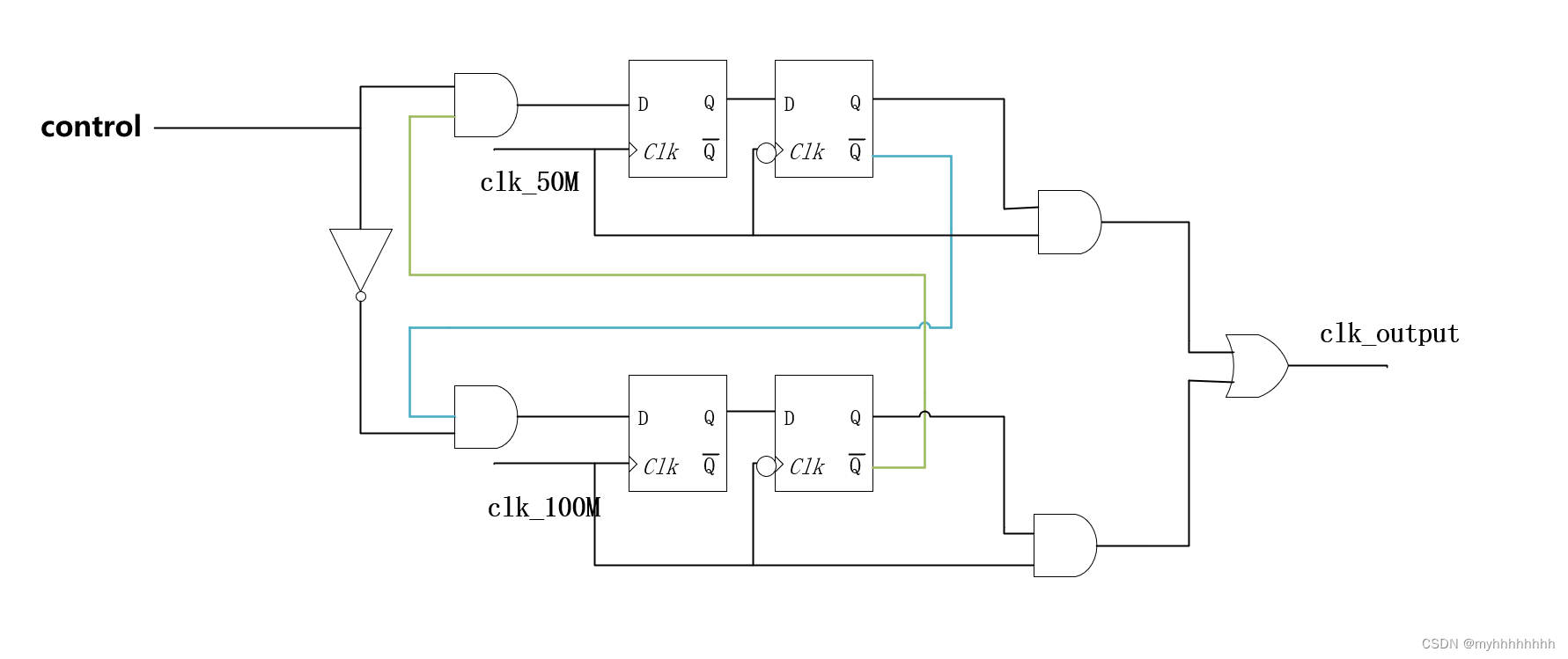
- control Whether the signal passes from above or below , Both go through two levels of sampling , Metastable state is avoided
- The next level DFF Sample with falling edge , Avoid the occurrence of sampling burrs
- Level second DFF Of not Q The logic of returns the input in the form of negative feedback , Take and logic , Build up 50M The clock and 100M The relationship between clocks , It means before switching The clock waited for a while , Will switch to the clock after switching , Avoid switching burrs
- Finally, the upper circuit and the lower circuit , With Or logic Phase extraction , Output clk_output.
Four 、RTL Design
module free_glitch(clk_50M,clk_100M,control,rst_n,clk_output);
input clk_50M; // clock with 50M frequency
input clk_100M; // clock with 100M frequency
input control; // control signal
input rst_n; // reset signal
output clk_output; // output clock

reg clk_50_r1; // register for 50M clock
reg clk_50_r2;
reg clk_100_r1;// register for 100M clock
reg clk_100_r2;

wire logic_50_ctl; // logic "and" before DFF_r1 for 50M clock
wire logic_100_ctl; // logic "and" before DFF_r2 for 100M clock

assign logic_50_ctl  =  control & !clk_100_r2; // generate logic
assign logic_100_ctl = !control & !clk_50_r2; // generate logic


[email protected](posedge clk_50M or negedge rst_n)
	if(!rst_n)
		clk_50_r1 <= 1'b0;
	else
		clk_50_r1 <= logic_50_ctl;

[email protected](negedge clk_50M or negedge rst_n)
	if(!rst_n)
		clk_50_r2 <= 1'b0;
	else
		clk_50_r2 <= clk_50_r1;

[email protected](posedge clk_100M or negedge rst_n)
	if(!rst_n)
		clk_100_r1 <= 1'b0;
	else
		clk_100_r1 <= logic_100_ctl;


[email protected](negedge clk_100M or negedge rst_n)
	if(!rst_n)
		clk_100_r2 <= 1'b0;
	else
		clk_100_r2 <= clk_100_r1;

assign clk_output = (clk_100_r2&clk_100M) | (clk_50_r2&clk_50M ); // generate final signal clock output

endmodule
5、 ... and 、 Simulation
`timescale 1ns / 1ps
module free_glitch_tb();
reg clk_50M;
reg clk_100M;
reg control;
reg rst_n;
wire clk_output;

free_glitch u1(clk_50M,clk_100M,control,rst_n,clk_output);

always #5 clk_100M = !clk_100M;
always #10 clk_50M = !clk_50M;

initial
begin
clk_100M = 0;
clk_50M = 1;
rst_n = 1;
control = 1;
#100
rst_n = 0;
#50
rst_n = 1;
#100
control =0;
#100
control =1;
#128
control = 0;

end


endmodule
6、 ... and 、 Simulation analysis
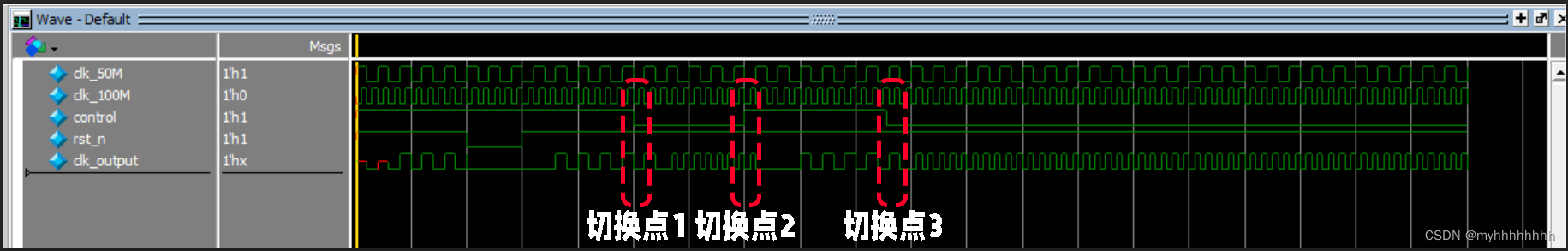
We can find out , When control After change , For a while delay when , The clock signal is Switch to the clock of the target , It is the appearance of this delay , Ensure that there are no burrs , The design meets the requirements
边栏推荐
- Assembly and Interface Technology Experiment 6 - ADDA conversion experiment, AD acquisition system in interrupt mode
- [10:00 public class]: basis and practice of video quality evaluation
- ResNet-RS:谷歌领衔调优ResNet,性能全面超越EfficientNet系列 | 2021 arxiv
- AI 企业多云存储架构实践 | 深势科技分享
- Realization of epoll reactor model
- MariaDb数据库管理系统的学习(一)安装示意图
- China 1,4-cyclohexanedimethanol (CHDM) industry research and investment decision-making report (2022 Edition)
- GPS from getting started to giving up (12), Doppler constant speed
- Qt | UDP广播通信、简单使用案例
- 保存和检索字符串
猜你喜欢
Xiaoman network model & http1-http2 & browser cache
Management background --3, modify classification

C # réalise la liaison des données du rapport Crystal et l'impression du Code à barres 4
Management background --5, sub classification
GPS from entry to abandonment (XVII), tropospheric delay
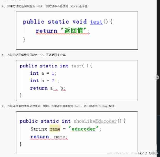
Method return value considerations
GPS from getting started to giving up (16), satellite clock error and satellite ephemeris error

Common sense: what is "preservation" in insurance?
![Some problems about the use of char[] array assignment through scanf..](/img/cf/d85a3172c5d29ac00377f9c30dbc4f.png)
Some problems about the use of char[] array assignment through scanf..

GNN,请你的网络层数再深一点~
随机推荐
CCNA-思科网络 EIGRP协议
Oracle性能分析3:TKPROF简介
[10:00 public class]: basis and practice of video quality evaluation
What a new company needs to practice and pay attention to
保存和检索字符串
Management background --2 Classification list
MariaDB database management system learning (I) installation diagram
Leetcode question brushing (XI) -- sequential questions brushing 51 to 55
二叉(搜索)树的最近公共祖先 ●●
[sdx62] wcn685x will bdwlan Bin and bdwlan Txt mutual conversion operation method
Data processing skills (7): MATLAB reads the data in the text file TXT with mixed digital strings
Common sense: what is "preservation" in insurance?
微信红包封面小程序源码-后台独立版-带测评积分功能源码
[sciter bug] multi line hiding
12、 Start process
GPS從入門到放弃(十三)、接收機自主完好性監測(RAIM)
Yyds dry goods inventory C language recursive implementation of Hanoi Tower
HDU 2008 数字统计
BarcodeX(ActiveX打印控件) v5.3.0.80 免费版使用
小满网络模型&http1-http2 &浏览器缓存