当前位置:网站首页>Mcp4725 driver based on FPGA
Mcp4725 driver based on FPGA
2020-11-10 10:46:00 【I don't know.】
be based on FPGA Of MCP4725 The driver
- Chip data
MCP4725 It's low power 、 High precision 、 Single channel 12 Bit buffer voltage output DAC (Digital-to-Analog Convertor,DAC), With nonvolatile memory (EEPROM). Users can use I2C The interface command will DAC Input and configuration data are written to nonvolatile memory (EEPROM). The nonvolatile memory function makes DAC The device can maintain during power failure DAC Enter the code , And DAC The output is available immediately after power up .
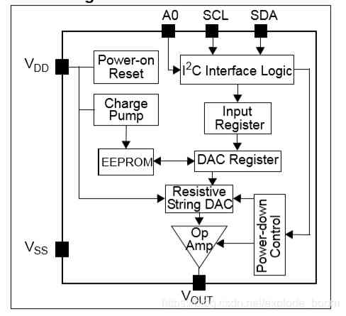
chart 1.MCP4725 Functional block diagram
MCP4725 Having external A0 Address bit selection pin . this A0 Pins can be connected to the user's application board VDD or VSS.MCP4725 have 2 Linetype IIC Compatible with serial interface , Can be used for standard (100 kHz)、 Fast (400 kHz) Or high speed (3.4 MHz) Pattern .
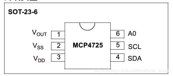
Vout: Analog output voltage ;
Vss: Reference point ;
VDD: Supply voltage ;3.7~5.5V
SDA:IIC Serial data ;
SCL:IIC Serial clock input
A0: Address bit selection pin ; The pin can be connected to VSS or VDD , Or effectively driven by digital logic level . The logical state of the pin determines I2 C Address bit A0 position .
2. Output voltage calculation
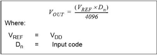
For example, when we type 0x400, It's a decimal number 1024, The power supply voltage is connected to 5V, So the output voltage Vout=5*1024/4096=1.25V.
3. working principle
When the device is connected to I2C Bus time , The device works as a slave device . Use I2C Interface command , The main device can read / Write DAC Input register or EEPROM.MCP4725 The device address contains 4 A fixed position (1100 = Device code ) and 3 Address bits (A2、A1 and A0).A2 and A1 Bits are hardwired at the factory , and A0 Bitwise by A0 The logical state of the pin determines .A0 Pins can be connected to VDD or VSS, Or effectively driven by digital logic level . The write command is used to combine the configuration bit with DAC Input code to load into DAC register , Or writing devices EEPROM. By using 3 Write command type bits (C2、C1 and C0) Define the type of write command .
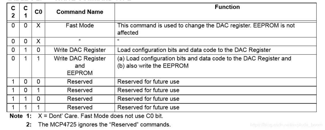
When C2=0,C1=0 when , For fast mode , This command is used to change DAC register ,EEPROM Unaffected ; When C2=0,C1=1,C0=0 when , For writing DAC Register mode , Load configuration bits and data code to DAC register ; When C2=0,C1=1,C0=1 when , For writing DAC Registers and updates EEPROM Pattern , Load the configuration bits and data code to DAC Register and write EEPROM in . This time I mainly use to write DAC Register mode and write DAC Registers and updates EEPROM Pattern , As shown in the figure below .
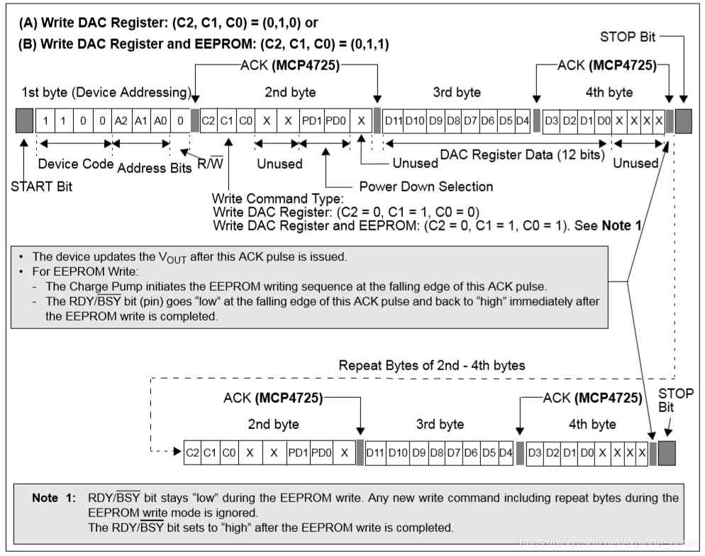
The first byte is device addressing ,A2 and A1 It has been set by the manufacturer to 0,A0 Self control ( The default is 0, That is, grounding ), So the first byte is 0x60; The second byte is the write data address ,PD0 and PD1 All for 0 It's normal mode , So the second byte is 0x60; The height of the third and fourth bytes 4 A composition 12 Bit data input , It's up to us to define the input .
4. IIC serial communication
MCP4725 The device uses 2 Line IIC serial interface , The interface is available in standard 、 Working in fast or high speed mode . The device that sends data on the bus is defined as a transmitter , The device that receives data is defined as a receiver . The bus must be controlled by the master device , When the main device generates serial (SCL) The signal 、 Control bus access and generate start and stop conditions .MCP4725 The device works as a slave device . Both master and slave devices can work as transmitters or receivers , But it's up to the master to decide which mode to activate . Communication is made up of a master device ( Single chip microcomputer ) launch , It sends the start bit , Followed by the address byte . The first byte sent is always the slave address byte , It contains the device code 、 Address bits and R/W position .MCP4725 The device code of the device is 1100. When the device receives a read command (R/W = 1) when , send out DAC Input registers and EEPROM The content of . The figure below shows IIC Communication timing requirements .

In this design ,SCL The clock input frequency is selected as 250KHz,FPGA The working clock is 50MHz, Power on and wait 20ms Later on IIC Data writing . Modular design , It is divided into IIC Drive design ,MCP4725 Initialization design , Top level modules .
5. Code module
5.1 IIC Driver module
module i2c_dri
#(// slave address( Device address )
parameter SLAVE_ADDR = 7'b1100000 ,
parameter CLK_FREQ = 26'd50_000_000, // clock frequency (CLK_FREQ)
parameter I2C_FREQ = 18'd250_000 // I2C Of SCL clock frequency
)(
//global clock
input clk , // The clock
input rst_n , // Reset signal
//i2c interface
input i2c_exec , // I2C Trigger execution signal
input bit_ctrl , // Word address bit control (16b/8b)
input i2c_rh_wl , // I2C Read write control signal
input [15:0] i2c_addr , // I2C Address in device
input [15:0] i2c_data_w , // I2C Data to write
output reg [ 7:0] i2c_data_r , // I2C Read out data
output reg i2c_done , // I2C One operation complete
output reg scl , // I2C Of SCL Clock signal
inout sda , // I2C Of SDA The signal
//user interface
output reg dri_clk // drive I2C Operating drive clock
);
//localparam define
localparam st_idle = 8'b0000_0001; // Idle state
localparam st_sladdr = 8'b0000_0010; // Send device address (slave address)
localparam st_addr16 = 8'b0000_0100; // send out 16 Bit word address
localparam st_addr8 = 8'b0000_1000; // send out 8 Bit word address
localparam st_data_wr = 8'b0001_0000; // Writing data (8 bit)
localparam st_addr_rd = 8'b0010_0000; // Send device address read
localparam st_data_rd = 8'b0100_0000; // Reading data (8 bit)
localparam st_stop = 8'b1000_0000; // end I2C operation
//reg define
reg sda_dir ; // I2C data (SDA) Direction control
reg sda_out ; // SDA The output signal
reg st_done ; // State end
reg wr_flag ; // Write a sign
reg [ 6:0] cnt ; // Count
reg [ 7:0] cur_state ; // State machine current state
reg [ 7:0] next_state ; // State machine next state
reg [15:0] addr_t ; // Address
reg [ 7:0] data_r ; // Read data
reg [15:0] data_wr_t ; // I2C Temporary deposit of data to be written
reg [ 9:0] clk_cnt ; // Divide the clock count
//wire define
wire sda_in ; // SDA Input signal
wire [8:0] clk_divide ; // The division coefficient of the module driven clock
//SDA control
assign sda = sda_dir ? sda_out : 1'bz; // SDA Data output or high resistance
assign sda_in = sda ; // SDA data input
assign clk_divide = (CLK_FREQ/I2C_FREQ) >> 3; // The division coefficient of the module driven clock
// Generate I2C Of SCL Four times the frequency of the drive clock is used to drive i2c The operation of
always @(posedge clk or negedge rst_n) begin
if(!rst_n) begin
dri_clk <= 1'b1;
clk_cnt <= 10'd0;
end
else if(clk_cnt == clk_divide - 1'd1) begin
clk_cnt <= 10'd0;
dri_clk <= ~dri_clk;
end
else
clk_cnt <= clk_cnt + 1'b1;
end
//( Three stage state machine ) Synchronous timing describes state transitions
always @(posedge dri_clk or negedge rst_n) begin
if(!rst_n)
cur_state <= st_idle;
else
cur_state <= next_state;
end
// Combinational logic determines the condition of state transition
always @( * ) begin
// next_state = st_idle;
case(cur_state)
st_idle: begin // Idle state
if(i2c_exec) begin
next_state = st_sladdr;
end
else
next_state = st_idle;
end
st_sladdr: begin
if(st_done) begin
if(bit_ctrl) // Judgment is 16 A still 8 Bit word address
next_state = st_addr16;
else
next_state = st_addr8 ;
end
else
next_state = st_sladdr;
end
st_addr16: begin // Write 16 Bit word address
if(st_done) begin
next_state = st_addr8;
end
else begin
next_state = st_addr16;
end
end
st_addr8: begin // 8 Bit word address
if(st_done) begin
if(wr_flag==1'b0) // Read and write
next_state = st_data_wr;
else
next_state = st_addr_rd;
end
else begin
next_state = st_addr8;
end
end
st_data_wr: begin // Writing data (8 bit)
if(st_done)
next_state = st_stop;
else
next_state = st_data_wr;
end
st_addr_rd: begin // Write an address to read data
if(st_done) begin
next_state = st_data_rd;
end
else begin
next_state = st_addr_rd;
end
end
st_data_rd: begin // Reading data (8 bit)
if(st_done)
next_state = st_stop;
else
next_state = st_data_rd;
end
st_stop: begin // end I2C operation
if(st_done)
next_state = st_idle;
else
next_state = st_stop ;
end
default: next_state= st_idle;
endcase
end
// Sequential circuits describe state outputs
always @(posedge dri_clk or negedge rst_n) begin
// Reset initialization
if(!rst_n) begin
scl <= 1'b1;
sda_out <= 1'b1;
sda_dir <= 1'b1;
i2c_done <= 1'b0;
cnt <= 1'b0;
st_done <= 1'b0;
data_r <= 1'b0;
i2c_data_r <= 1'b0;
wr_flag <= 1'b0;
addr_t <= 1'b0;
data_wr_t <= 1'b0;
end
else begin
st_done <= 1'b0 ;
cnt <= cnt +1'b1 ;
case(cur_state)
st_idle: begin // Idle state
scl <= 1'b1;
sda_out <= 1'b1;
sda_dir <= 1'b1;
i2c_done<= 1'b0;
cnt <= 7'b0;
if(i2c_exec) begin
wr_flag <= i2c_rh_wl ;
addr_t <= i2c_addr ;
data_wr_t <= i2c_data_w;
end
end
st_sladdr: begin // Write the address ( Device address and word address )
case(cnt)
7'd1 : sda_out <= 1'b0; // Start I2C
7'd3 : scl <= 1'b0;
7'd4 : sda_out <= SLAVE_ADDR[6]; // Send device address
7'd5 : scl <= 1'b1;
7'd7 : scl <= 1'b0;
7'd8 : sda_out <= SLAVE_ADDR[5];
7'd9 : scl <= 1'b1;
7'd11: scl <= 1'b0;
7'd12: sda_out <= SLAVE_ADDR[4];
7'd13: scl <= 1'b1;
7'd15: scl <= 1'b0;
7'd16: sda_out <= SLAVE_ADDR[3];
7'd17: scl <= 1'b1;
7'd19: scl <= 1'b0;
7'd20: sda_out <= SLAVE_ADDR[2];
7'd21: scl <= 1'b1;
7'd23: scl <= 1'b0;
7'd24: sda_out <= SLAVE_ADDR[1];
7'd25: scl <= 1'b1;
7'd27: scl <= 1'b0;
7'd28: sda_out <= SLAVE_ADDR[0];
7'd29: scl <= 1'b1;
7'd31: scl <= 1'b0;
7'd32: sda_out <= 1'b0; // 0: Write
7'd33: scl <= 1'b1;
7'd35: scl <= 1'b0;
7'd36: begin
sda_dir <= 1'b0; // Slave response
sda_out <= 1'b1;
end
7'd37: scl <= 1'b1;
7'd38: st_done <= 1'b1;
7'd39: begin
scl <= 1'b0;
cnt <= 1'b0;
end
default : ;
endcase
end
st_addr16: begin
case(cnt)
7'd0 : begin
sda_dir <= 1'b1 ;
sda_out <= addr_t[15]; // Send word address
end
7'd1 : scl <= 1'b1;
7'd3 : scl <= 1'b0;
7'd4 : sda_out <= addr_t[14];
7'd5 : scl <= 1'b1;
7'd7 : scl <= 1'b0;
7'd8 : sda_out <= addr_t[13];
7'd9 : scl <= 1'b1;
7'd11: scl <= 1'b0;
7'd12: sda_out <= addr_t[12];
7'd13: scl <= 1'b1;
7'd15: scl <= 1'b0;
7'd16: sda_out <= addr_t[11];
7'd17: scl <= 1'b1;
7'd19: scl <= 1'b0;
7'd20: sda_out <= addr_t[10];
7'd21: scl <= 1'b1;
7'd23: scl <= 1'b0;
7'd24: sda_out <= addr_t[9];
7'd25: scl <= 1'b1;
7'd27: scl <= 1'b0;
7'd28: sda_out <= addr_t[8];
7'd29: scl <= 1'b1;
7'd31: scl <= 1'b0;
7'd32: begin
sda_dir <= 1'b0; // Slave response
sda_out <= 1'b1;
end
7'd33: scl <= 1'b1;
7'd34: st_done <= 1'b1;
7'd35: begin
scl <= 1'b0;
cnt <= 1'b0;
end
default : ;
endcase
end
st_addr8: begin
case(cnt)
7'd0: begin
sda_dir <= 1'b1 ;
sda_out <= addr_t[7]; // Word address
end
7'd1 : scl <= 1'b1;
7'd3 : scl <= 1'b0;
7'd4 : sda_out <= addr_t[6];
7'd5 : scl <= 1'b1;
7'd7 : scl <= 1'b0;
7'd8 : sda_out <= addr_t[5];
7'd9 : scl <= 1'b1;
7'd11: scl <= 1'b0;
7'd12: sda_out <= addr_t[4];
7'd13: scl <= 1'b1;
7'd15: scl <= 1'b0;
7'd16: sda_out <= addr_t[3];
7'd17: scl <= 1'b1;
7'd19: scl <= 1'b0;
7'd20: sda_out <= addr_t[2];
7'd21: scl <= 1'b1;
7'd23: scl <= 1'b0;
7'd24: sda_out <= addr_t[1];
7'd25: scl <= 1'b1;
7'd27: scl <= 1'b0;
7'd28: sda_out <= addr_t[0];
7'd29: scl <= 1'b1;
7'd31: scl <= 1'b0;
7'd32: begin
sda_dir <= 1'b0; // Slave response
sda_out <= 1'b1;
end
7'd33: scl <= 1'b1;
7'd34: st_done <= 1'b1;
7'd35: begin
scl <= 1'b0;
cnt <= 1'b0;
end
default : ;
endcase
end
st_data_wr: begin // Writing data (12 bit)
case(cnt)
7'd0: begin
sda_out <= data_wr_t[15]; // I2C Write 2 Time 8 Bit data
sda_dir <= 1'b1;
end
7'd1 : scl <= 1'b1;
7'd3 : scl <= 1'b0;
7'd4 : sda_out <= data_wr_t[14];
7'd5 : scl <= 1'b1;
7'd7 : scl <= 1'b0;
7'd8 : sda_out <= data_wr_t[13];
7'd9 : scl <= 1'b1;
7'd11: scl <= 1'b0;
7'd12: sda_out <= data_wr_t[12];
7'd13: scl <= 1'b1;
7'd15: scl <= 1'b0;
7'd16: sda_out <= data_wr_t[11];
7'd17: scl <= 1'b1;
7'd19: scl <= 1'b0;
7'd20: sda_out <= data_wr_t[10];
7'd21: scl <= 1'b1;
7'd23: scl <= 1'b0;
7'd24: sda_out <= data_wr_t[9];
7'd25: scl <= 1'b1;
7'd27: scl <= 1'b0;
7'd28: sda_out <= data_wr_t[8];
7'd29: scl <= 1'b1;
7'd31: scl <= 1'b0;
7'd32: begin
sda_dir <= 1'b0; // Slave response
sda_out <= 1'b1;
end
7'd33: scl <= 1'b1;
7'd35: scl <= 1'b0;
7'd36: sda_out <= data_wr_t[7];
7'd37: scl <= 1'b1;
7'd39: scl <= 1'b0;
7'd40: sda_out <= data_wr_t[6];
7'd41: scl <= 1'b1;
7'd43: scl <= 1'b0;
7'd44: sda_out <= data_wr_t[5];
7'd45: scl <= 1'b1;
7'd47: scl <= 1'b0;
7'd48: sda_out <= data_wr_t[4];
7'd49: scl <= 1'b1;
7'd51: scl <= 1'b0;
7'd52: sda_out <= data_wr_t[3];
7'd53: scl <= 1'b1;
7'd55: scl <= 1'b0;
7'd56: sda_out <= data_wr_t[2];
7'd57: scl <= 1'b1;
7'd59: scl <= 1'b0;
7'd60: sda_out <= data_wr_t[1];
7'd61: scl <= 1'b1;
7'd63: scl <= 1'b0;
7'd64: sda_out <= data_wr_t[0];
7'd65: scl <= 1'b1;
7'd67: scl <= 1'b0;
7'd68: begin
sda_dir <= 1'b0; // Slave response
sda_out <= 1'b1;
end
7'd69: scl <= 1'b1;
7'd70: st_done <= 1'b1;
7'd71: begin
scl <= 1'b0;
cnt <= 1'b0;
end
default : ;
endcase
end
st_addr_rd: begin // Write an address to read data
case(cnt)
7'd0 : begin
sda_dir <= 1'b1;
sda_out <= 1'b1;
end
7'd1 : scl <= 1'b1;
7'd2 : sda_out <= 1'b0; // restart
7'd3 : scl <= 1'b0;
7'd4 : sda_out <= SLAVE_ADDR[6]; // Send device address
7'd5 : scl <= 1'b1;
7'd7 : scl <= 1'b0;
7'd8 : sda_out <= SLAVE_ADDR[5];
7'd9 : scl <= 1'b1;
7'd11: scl <= 1'b0;
7'd12: sda_out <= SLAVE_ADDR[4];
7'd13: scl <= 1'b1;
7'd15: scl <= 1'b0;
7'd16: sda_out <= SLAVE_ADDR[3];
7'd17: scl <= 1'b1;
7'd19: scl <= 1'b0;
7'd20: sda_out <= SLAVE_ADDR[2];
7'd21: scl <= 1'b1;
7'd23: scl <= 1'b0;
7'd24: sda_out <= SLAVE_ADDR[1];
7'd25: scl <= 1'b1;
7'd27: scl <= 1'b0;
7'd28: sda_out <= SLAVE_ADDR[0];
7'd29: scl <= 1'b1;
7'd31: scl <= 1'b0;
7'd32: sda_out <= 1'b1; // 1: read
7'd33: scl <= 1'b1;
7'd35: scl <= 1'b0;
7'd36: begin
sda_dir <= 1'b0; // Slave response
sda_out <= 1'b1;
end
7'd37: scl <= 1'b1;
7'd38: st_done <= 1'b1;
7'd39: begin
scl <= 1'b0;
cnt <= 1'b0;
end
default : ;
endcase
end
st_data_rd: begin // Reading data (8 bit)
case(cnt)
7'd0: sda_dir <= 1'b0;
7'd1: begin
data_r[7] <= sda_in;
scl <= 1'b1;
end
7'd3: scl <= 1'b0;
7'd5: begin
data_r[6] <= sda_in ;
scl <= 1'b1 ;
end
7'd7: scl <= 1'b0;
7'd9: begin
data_r[5] <= sda_in;
scl <= 1'b1 ;
end
7'd11: scl <= 1'b0;
7'd13: begin
data_r[4] <= sda_in;
scl <= 1'b1 ;
end
7'd15: scl <= 1'b0;
7'd17: begin
data_r[3] <= sda_in;
scl <= 1'b1 ;
end
7'd19: scl <= 1'b0;
7'd21: begin
data_r[2] <= sda_in;
scl <= 1'b1 ;
end
7'd23: scl <= 1'b0;
7'd25: begin
data_r[1] <= sda_in;
scl <= 1'b1 ;
end
7'd27: scl <= 1'b0;
7'd29: begin
data_r[0] <= sda_in;
scl <= 1'b1 ;
end
7'd31: scl <= 1'b0;
7'd32: begin
sda_dir <= 1'b1; // Non response
sda_out <= 1'b1;
end
7'd33: scl <= 1'b1;
7'd34: st_done <= 1'b1;
7'd35: begin
scl <= 1'b0;
cnt <= 1'b0;
i2c_data_r <= data_r;
end
default : ;
endcase
end
st_stop: begin // end I2C operation
case(cnt)
7'd0: begin
sda_dir <= 1'b1; // end I2C
sda_out <= 1'b0;
end
7'd1 : scl <= 1'b1;
7'd3 : sda_out <= 1'b1;
7'd15: st_done <= 1'b1;
7'd16: begin
cnt <= 1'b0;
i2c_done <= 1'b1; // Pass to upper module I2C End signal
end
default : ;
endcase
end
endcase
end
end
endmodule
5.2 MCP4725 Initialization module
module MCP4725_init(

    input                clk      ,   // Clock signal
    input                rst_n    ,   // Reset signal , Low level active

    input                i2c_done ,   //I2C Register configuration completion signal
    output  reg          i2c_exec ,   //I2C Trigger execution signal
    output  reg  [23:0]  i2c_data    //I2C Address and data to be configured ( high 16 Bit address , low 8 Bit data )
);


//reg define
reg   [14:0]   start_init_cnt;        // Wait for the delay counter


//scl configure 250khz, Input clk by 1Mhz, The period is 1us,20000*1us = 20ms
// Power on to start configuration IIC At least wait for 20ms
always @(posedge clk or negedge rst_n) begin
    if(!rst_n)
        start_init_cnt <= 15'd0;
    else if(start_init_cnt < 15'd20000)
        start_init_cnt <= start_init_cnt + 1'b1;
end


//i2c Trigger execution signal
always @(posedge clk or negedge rst_n) begin
    if(!rst_n)
        i2c_exec <= 1'b0;
    else if(start_init_cnt == 15'd19999)
        i2c_exec <= 1'b1;

    else
        i2c_exec <= 1'b0;
end


// Configure register address and data
always @(posedge clk or negedge rst_n) begin
    if(!rst_n)
        i2c_data <= 16'd0;
	 else
	     i2c_data <= {

   8'h60,8'h40,8'h00} ;// The first byte is mode control (60: Update to EEPROM;40: Update only DAC register ), The next two bytes are input data , Take the height 12 position

	 end
endmodule
5.3 Top level modules
module MCP4725_CTRL(

  input clk,
  input rst_n,

  output scl,
  inout sda

);

  wire                  i2c_exec        ;  //I2C Trigger execution signal
  wire   [23:0]         i2c_data        ;  //I2C Address and data to be configured ( high 8 Bit address , low 16 Bit data )
  wire                  i2c_done        ;  //I2C Register configuration completion signal
  wire                  i2c_dri_clk     ;  //I2C Operating the clock

  parameter  SLAVE_ADDR = 7'h60         ;  //MCP4725 The device address of 7'h60
  parameter  BIT_CTRL   = 1'b0          ;  // Byte address is 8 position   0:8 position  1:16 position
  parameter  CLK_FREQ   = 26'd50_000_000;  // clock frequency  50MHz
  parameter  I2C_FREQ   = 18'd250_000   ;  //I2C Of SCL clock frequency ,250KHz


 i2c_dri
   #(
    .SLAVE_ADDR         (SLAVE_ADDR),       // Parameter passing
    .CLK_FREQ           (CLK_FREQ  ),
    .I2C_FREQ           (I2C_FREQ  )
    )
   u_i2c_dri(
    .clk                (clk       ),
    .rst_n              (rst_n     ),

    .i2c_exec           (i2c_exec  ),
    .bit_ctrl           (BIT_CTRL  ),
    .i2c_rh_wl          (1'b0),             // Fixed for 0, It's only used. IIC Driven write operations
    .i2c_addr           (i2c_data[23:16]),
    .i2c_data_w         (i2c_data[15:0]),
    .i2c_data_r         (),
    .i2c_done           (i2c_done  ),
    .scl                (scl   ),
    .sda                (sda   ),

    .dri_clk            (i2c_dri_clk)       //I2C Operating the clock
);

MCP4725_init u_MCP4725_init(

   .clk     (i2c_dri_clk),   // Clock signal
   .rst_n   (rst_n),   // Reset signal , Low level active
   .i2c_done(i2c_done),   //I2C Register configuration completion signal
   .i2c_exec(i2c_exec),   //I2C Trigger execution signal
   .i2c_data(i2c_data)   //I2C Address and data to be configured ( high 8 Bit address , low 16 Bit data )
);


endmodule
PS:IIC I wrote the driver before IIC Based on the single byte read-write program , So as to realize the writing of two bytes ( Here you can add multiple byte write , But should pay attention to cnt The bit width of ).MCP4725 The last... In the initialization program i2c_data <= {8’h60,8’h40,8’h00} ; You can make changes in this line according to your actual needs , Please refer to the data manual of the chip for details .
6. verification
After compiling the project sof Download the file to EP4CE6F17C8 In the device , Well connected MCP4725 Each pin , The power supply is connected to 5V, The data entered is 1024, by 4096 Quarter of , So the output voltage should be 1.25V, Using a multimeter, the measured data is 1.25V, Power off the module and power it on again , The second measurement is also 1.25V, Prove that the data was successfully written to EEPROM in , Verify success .
版权声明
本文为[I don't know.]所创,转载请带上原文链接,感谢
边栏推荐
- csdn bug7:待加
- [paper reading notes] rosane, robust and scalable attributed network embedding for sparse networks
- What can I do if I can't register didi? How to deal with it?
- 一不小心画了 24 张图剖析计网应用层协议!
- Android quick shutdown app
- Getiservicemanager () source code analysis
- python pip命令的使用
- On fedlearner, the latest open source federated machine learning platform of byte
- [论文阅读笔记] A Multilayered Informative Random Walk for Attributed Social Network Embedding
- Q & A and book donation activities of harbor project are in hot progress
猜你喜欢

高通骁龙875夺安卓处理器桂冠,但外挂5G基带成为它的弊病

MultiBank Group宣布创纪录的财务业绩,2020年前三季度毛利达到9,400万美元

2020-11-07

Design mode (8) -- command mode

learning to Estimate 3D Hand Pose from Single RGB Images论文理解
Sign in with apple
Swoole 如何使用 Xdebug 进行单步调试

To speed up the process of forming a global partnership between lifech and Alibaba Group
Looking for a small immutable dictionary with better performance

Understanding of learning to estimate 3D hand pose from single RGB images
随机推荐
CCR炒币机器人:新冠肺炎加速了监管机构对CBDC的兴趣
On fedlearner, the latest open source federated machine learning platform of byte
区块链论文集【三十一】
He doubled the fluency of the long list of idle fish app
GNU assembly language uses inline assembly to extend ASM
File初相识
[paper reading notes] rosane, robust and scalable attributed network embedding for sparse networks
gnu汇编语言使用内联汇编 扩展asm
Getiservicemanager () source code analysis
Hystrix 如何解决 ThreadLocal 信息丢失
他把闲鱼APP长列表流畅度翻了倍
从大专生到蚂蚁金服CTO,他写下“支付宝”第一行代码:逆风的方向,更适合飞翔!...
gnu汇编-基本数学方程-乘法
Only options request is sent, no post solution is sent
基于FPGA的MCP4725驱动程序
To speed up the process of forming a global partnership between lifech and Alibaba Group
刷题到底有什么用?你这么刷题还真没用
csdn bug5:待加
csdn bug7:待加
Design mode (8) -- command mode