当前位置:网站首页>Mipi interface, DVP interface and CSI interface of camera
Mipi interface, DVP interface and CSI interface of camera
2022-07-05 06:54:00 【Enlaihe】
The computer camera interface is USB Interface , The camera interface of smartphone is MIPI Interface , There are also some cameras ( For example, some support DVP Interface hardware ) yes DVP Interface .
USB It's a universal serial bus (Universal Serial Bus) For short , and MIPI Is the mobile industry processor interface (Mobile Industry Processor Interface),DVP It's a digital video port (digital video port) For short ,CSI Camera serial interface (CMOS Sensor Interface) For short .
Camera How it works
working process
The outside light passes through lens after , after color filter After filtering, it irradiates Sensor On the surface ,Sensor Will be taken from lens The transmitted light is converted into an electrical signal , And then through the inside AD Convert to digital signals . If Sensor No set become DSP, Through DVP Transfer to baseband, At this time, the data format is RAW DATA. If integration 了 DSP, RAW DATA Data after AWB、 be color matrix、 lens shading、 gamma、 sharpness、 AE and de-noise Handle , Post output YUV perhaps RGB Formatted data .
Finally by CPU Deliver to framebuffer It shows that , So you can see camera The scene taken .
Camera Main components
camera Mainly from lens and sensor IC Two parts , Some of them sensor IC Integrate 了 DSP, Some are not integrated , But it also requires external DSP Handle .camera It consists of the following parts :
lens( The lens ) commonly camera The lens structure is composed of several lenses , There are plastic lenses (Plastic) And glass mirror (Glass)
, Usually the lens structure has :1P,2P,1G1P,1G3P,2G2P,4G etc. .
sensor( image sensor ) Senor It's a semiconductor chip , There are two types of :CCD(Charge Coupled Device) Abbreviation for charge coupled device and CMOS(Complementary Metal-Oxide Semiconductor) Complementary metal oxide semiconductor .
CCD sensor , The charge signal is transmitted first , Post amplification , Again A/D, High imaging quality and sensitivity 、 Good resolution 、 Small noise ; Slow processing speed ; High cost , Process complex .
CMOS sensor , The charge signal is amplified first , after A/D, Retransmission ; Low imaging quality and sensitivity 、 Obvious noise ; Fast processing speed ; Low cost , Simple workmanship .
sensor Will be taken from lens The transmitted light is converted into an electrical signal , And then through the inside AD Convert to digital signals . because sensor Each pixel
Only light sensitive R Light or B Light or G light , So what each pixel stores at this time is monochromatic , We call it RAW DATA data .
Want to put each pixel's RAW DATA Restore data to three primary colors , Need ISP To deal with it . ISP( Image signal processing ) It mainly completes the processing of digital images , hold sensor Convert the collected raw data into display support The format of .
CAMIF(camera controller ) On the chip camera Interface circuit , Control the equipment , receive sensor Give the collected data to CPU, And send it to
LCD Display .
MIPI Interface
MIPI Cameras are common on mobile phones 、 In the plate , Support 500 High definition resolution of more than 10000 pixels . Its full name is “Mobile Industry Processor
Interface”, It is divided into MIPI DSI and MIPI CSI, Corresponding to video display and video input standards respectively . at present ,MIPI Camera in embedded products , Like dash cam 、 Law enforcement instrument 、 HD micro camera 、 Network monitoring cameras are widely used .
MIPI The definition of
MIPI union , Mobile industry processor interface (Mobile Industry Processor Interface abbreviation MIPI) union .
MIPI( Mobile industry processor interface ) yes MIPI An open standard and a specification for mobile application processors initiated by the alliance .
MIPI Characteristics
MIPI Differential serial transmission , Fast , anti-interference . Mainstream mobile phone modules now use MIPI transmission , Use... For transmission 4 Image data and a pair of differential clock signals are transmitted to the differential signal ; Originally to reduce LCD It is designed according to the number of wires between the screen and the main control chip , Later, it developed to high speed , Support high-resolution display , Now it's basically MIPI The interface .
MIPI The camera has three power supplies :VDDIO(IO Power Supply ),AVDD( Analog power ),DVDD( Core digital power supply ), Different sensor The camera power supply of the module is different
AVDD Yes 2.8V or 3.3V Of ;DVDD In general use 1.5V Or higher , Different manufacturers have different designs ,1.5V Maybe by sensor Module supply or external supply , If external power supply can be used, it is recommended to use external power supply , The voltage must be greater than the internal voltage DVDD;VDDIO The voltage should be equal to MIPI The level of the signal line is consistent , If the signal line is 2.8V level , be VDDIO Also available for 2.8V, There are some sensor The module can also not be used for VDDIO, Provided internally .
MIPI Of camera The interface is called CSI,MIPI Of display The interface is called DSI.
DVP
DVP Bus PCLK The limit is about 96M about , And the length of the line should not be too long , all DVP The maximum speed should be controlled at 72M following ,PCB layout Easier to draw
IPI Bus rate lvds Interface coupling , The routing must be differential equal length , And need protection , So yes PCB Wiring and impedance control requirements are higher ( Generally speaking, the differential impedance is required at 85 ohm ~125 Between ohms ).
DVP It's a parallel , need PCLK、VSYNC、HSYNC、D[0:11]—— It can be 8/10/12bit data , The specific situation depends on ISP or baseband Do you support
MIPI yes LVDS Low voltage differential serial port , Just need to CLKP/N、DATAP/N—— The biggest support 4-lane, commonly 2-lane It can be done
MIPI Interface than DVP There are few interface signal lines , Because it is a low-voltage differential signal , The interference is small , The anti-interference ability is also strong
DVP The interface is limited in terms of signal integrity , The rate is also limited .500W You can barely use DVP,800W And above MIPI Interface .
CSI Interface
Basic concepts
CSI-2 The interface specification is made up of MIPI(Mobile Industry Processor Interface) The alliance was organized in 2005 Camera serial interface released in , As a new interface framework between camera equipment and processor , Here you are 、 Mobile camera and other related industries provide a flexible and high-speed device interface [28]. before , Traditional camera interfaces generally include data bus 、 Clock bus 、 Synchronization signal line, control line, etc , The physical interface block diagram is shown below :

The physical interface of this camera occupies more data lines , The logic design is also complex , Horizontal synchronization signals are required , Vertical synchronization signal and clock signal , This puts forward higher requirements for the camera and the receiver
In the process of high-speed transmission , Directly using digital signals as data is easy to be disturbed by other external signals , Not as stable as the differential signal , This also greatly limits the transmission rate and the maximum image quality that the camera can transmit in real time .
be based on CSI-2 In the process of camera data transmission, the data differential signal is used to transmit the pixel value in the video , meanwhile CSI-2 The transmission interface can be simplified or expanded flexibly
For application scenarios with few interfaces ,CSI-2 The interface can only use a group of differential data signal lines and a group of differential clock lines to complete the data serial transmission process of the camera , This reduces the load , At the same time, it can also meet a certain transmission rate
For large arrays CCD The camera ,CSI-2 The interface can also extend its differential data line , So as to meet the high-speed requirements of parallel transmission of multiple groups of data lines .

CSI-2 The control interface is also integrated in the interface CCI(Camera Control Interface),CCI Is one that can support 400KHz Communication control interface of full duplex master-slave equipment with transmission rate , It can be compatible with many existing processors IIC Standard interface , Therefore, it is very convenient to realize Soc On CCI Master Module To CSI-2 TX End CCI Slave Module The control of
CSI Physical protocol layer provisions
MIPI In addition to new regulations on the interface of the camera, the alliance also stipulates CSI-2 The software architecture of the interface is further developed ,CSI-2 The software framework is mainly divided into three layers , They are application layer 、 Protocol layer 、 The physical layer , The protocol layer can be subdivided into pixel byte packaging layer / Decontamination layer 、LLP(Low LevelProtocol) layer 、 Channel management (Lane Management), The main system software block diagram is shown below :

CSI Protocol layer design :
application layer : It mainly designs the encoding and decoding format of the upper data stream , It specifies the mapping relationship between pixels and bytes ;
Protocol layer : It mainly includes pixels / Byte packing / Byte unpacking layer ,LLP Layer provides the synchronization mechanism of serial transmission data , The channel management layer provides data bit width scalability , So as to flexibly adapt to different application scenarios ;
The physical layer : Defines the basic transmission medium specification , To determine the CSI-2 Input and output characteristic parameters of protocol physical layer , And determine its electrical characteristics and clock timing .
in real life , Cameras can be seen everywhere , But for an electronic engineer , It is very necessary to understand the use of cameras , In general , The interfaces of the camera mainly include MIPI Interface 、DVP Interface 、CSI There are three types of interfaces , Let's talk about my understanding of these three categories .

Tools / raw material
Camera interface -MIPI、DVP、CSI
Method / step
Our commonly used computer camera interface is USB Interface , The common camera on smart phones is MIPI Interface , There are also some cameras ( For example, some support DVP Interface hardware ) yes DVP Interface ; Generally speaking ,USB It's a universal serial bus (Universal Serial Bus) For short , and MIPI Is the mobile industry processor interface (Mobile Industry Processor Interface),DVP It's a digital video port (digital video port) For short ,CSI Camera serial interface (CMOS Sensor Interface) For short .
DVP Bus PCLK The limit is about 96M about , And the length of the line should not be too long , all DVP The maximum speed should be controlled at 72M following ,PCB layout Easier to draw ;MIPI Bus rate lvds Interface coupling , The routing must be differential equal length , And need protection , So yes PCB Wiring and impedance control requirements are higher ( Generally speaking, the differential impedance is required at 85 ohm ~125 Between ohms ).
3
DVP It's a parallel , need PCLK、VSYNC、HSYNC、D[0:11]—— It can be 8/10/12bit data , The specific situation depends on ISP or baseband Do you support ;MIPI yes LVDS Low voltage differential serial port , Just need to CLKP/N、DATAP/N—— The biggest support 4-lane, commonly 2-lane It can be done .MIPI Interface than DVP There are few interface signal lines , Because it is a low-voltage differential signal , The interference is small , The anti-interference ability is also strong . most important of all DVP The interface is limited in terms of signal integrity , The rate is also limited .500W You can barely use DVP,800W And above MIPI Interface .
END
边栏推荐
- Volcano resource reservation feature
- Log4qt usage of logbase in QT project
- inux摄像头(mipi接口)简要说明
- 摄像头的MIPI接口、DVP接口和CSI接口
- Utf8 encoding
- [Chongqing Guangdong education] 1185t administrative leadership reference test of National Open University in autumn 2018
- Get class files and attributes by reflection
- The problem of Chinese garbled code in the vscode output box can be solved once for life
- Edge calculation data sorting
- PHY驱动调试之 --- PHY控制器驱动(二)
猜你喜欢
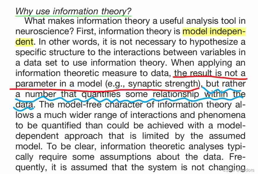
how to understand the “model independent.“

你心目中的数据分析 Top 1 选 Pandas 还是选 SQL?
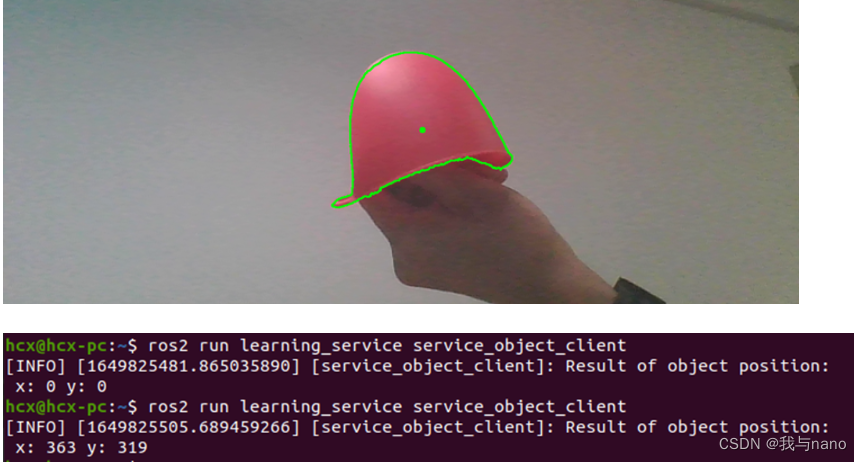
ROS2——Service服务(九)
睿智的目标检测59——Pytorch Focal loss详解与在YoloV4当中的实现
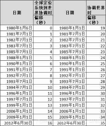
UTC, GPS time and Tai
【软件测试】04 -- 软件测试与软件开发
LSA Type Explanation - detailed explanation of lsa-2 (type II LSA network LSA) and lsa-3 (type III LSA network Summary LSA)
Vscode creates its own code template
Database mysql all
PHY驱动调试之 --- PHY控制器驱动(二)
随机推荐
A brief introduction to heading/pitch/roll and omega/phi/kappa
inux摄像头(mipi接口)简要说明
SD_CMD_SEND_SHIFT_REGISTER
2. Addition and management of Oracle data files
数学分析_笔记_第8章:重积分
Vscode configures the typera editor for MD
Ros2 - workspace (V)
Time is fast, please do more meaningful things
二分查找(折半查找)
Ros2 - first acquaintance with ros2 (I)
【软件测试】05 -- 软件测试的原则
The problem of Chinese garbled code in the vscode output box can be solved once for life
SRE核心体系了解
LSA Type Explanation - lsa-1 [type 1 LSA - router LSA] detailed explanation
Volcano resource reservation feature
ROS2——功能包(六)
Cookie、Session、JWT、token四者间的区别与联系
H5 embedded app adapts to dark mode
达梦数据库全部
ROS2——node节点(七)