当前位置:网站首页>SPI read / write flash principle + complete code
SPI read / write flash principle + complete code
2022-07-05 04:13:00 【Artemis_ yuer】
introduction
Realization SPI Communications , Yes FLASH To read and write . Read FLASH Of ID Information , Write data , And read it out for verification , Print the data written and read through the serial port , Output test results .
One 、SPI Bus
SPI The basics of communication
SPI It's a serial peripheral interface (Serial Peripheral Interface), Serial peripheral interface , It's a high speed full duplex communication bus , It is out of this simple and easy-to-use feature , Now more and more chips integrate this communication protocol , Maximum SPI Speed attainable 18MHz .
Usually SPI adopt 4 Pins are connected to external devices :
MISO: Master input / Output pin from device .
MOSI: Main device output / Input pins from the device .
SCK: Serial clock , Output as master device , Input from device .
NSS: Choose from the device . This is an optional pin , It's used to select the master / Slave device . Its function is to serve as a “ Clip selection pins ”, Let the master device communicate with a specific slave device independently , Avoid conflicts on data lines .
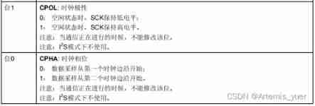
The phase and polarity of the clock signal
SPI_CR The register of CPOL and CPHA position , Can be combined into four possible temporal relationships , One of the most widely used is SPI0 and SPI3 The way .
SPI Module for data exchange with peripherals , According to the peripheral work requirements , Its output serial synchronous clock polarity and phase can be configured , Clock polarity (CPOL) There is no significant impact on the transmission protocol . If CPOL=0, The idle state of the serial synchronization clock is low ; If CPOL=1, The idle state of the serial synchronous clock is high level . Clock phase (CPHA) It can be configured to select one of two different transmission protocols for data transmission . If CPHA=0, At the first jump edge of the serial synchronization clock ( Up or down ) The data is sampled ; If CPHA=1, At the second jump edge of the serial synchronization clock ( Up or down ) The data is sampled .SPI The phase and polarity of the sound clock of the main module and the peripherals communicating with it shall be consistent .
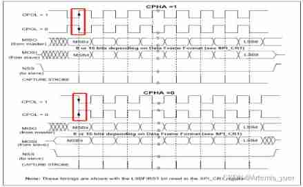
These time series reflect SPI_CR1 The register of LSBFIRST Reset ( Set up 0) The case when , namely MSB Pattern .
SPI Pattern | CPOL | CPHA | Idle SCK The clock | Sampling time |
0 | 0 | 0 | Low level | Odd edge |
1 | 0 | 1 | Low level | Even edge |
2 | 1 | 0 | High level | Odd edge |
3 | 1 | 1 | High level | Even edge |
SPI Main mode configuration
In the main configuration , The serial clock is SCK Foot generation , Learn to use registers , Understand the underlying logic ( It will also be clearer to develop with library functions ), The configuration steps are as follows :
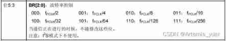
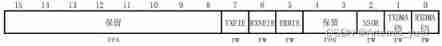
1、 adopt SPI_CR1 The register of BR[2:0] Bit defines serial clock baud rate .
SPI Control register 1(SPI_CR1)
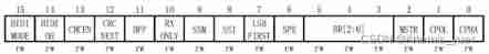
2、 choice CPOL and CPHA position , Define the phase relationship between data transmission and serial clock .
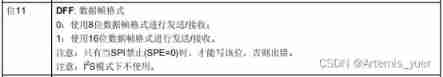
3、 Set up DFF To define 8 or 16 Bit data frame format .
4、 To configure SPI_CR1 The register of LSBFIRST Bit defines the frame format .

5、 If NSS The pin needs to work in input mode , In the hardware mode, during the whole data frame transmission, the NSS Feet connected to high level ; In software mode , Need to set up SPI_CR1 The register of SSM and SSI position .


6、 You have to set MSTR and SPE position ( should only NSS The pin is connected to high level , These bits can remain set ). In this configuration ,MOSI Feet are data output , and MISO Feet are data input .


 give an example :

void SPI1_Init(void)
{
    RCC->APB2ENR|=1<<2;  	    //PORTA Clock enable
    RCC->APB2ENR|=1<<12;   	    //SPI1 Clock enable
    GPIOA->CRL&=0X000FFFFF;     //PA5/6/7 Zero clearing
    GPIOA->CRL|=0XBBB00000;	    //PA5/6/7 Reuse
    GPIOA->ODR|=0X7<<5;         //PA5.6.7 Pull up
    GPIOA->CRL|=0X000000300;    //PA2 SPI The main device outputs
    SPI1->CR1|=0<<10;		    // Full duplex mode
    SPI1->CR1|=1<<9; 		    // Software NSS management
    SPI1->CR1|=1<<8;
    SPI1->CR1|=1<<2; 		    //SPI host
    SPI1->CR1|=0<<11;		    //8bit data format
    SPI1->CR1|=1<<1; 		    // In idle mode SCK by 1 CPOL=1
    SPI1->CR1|=1<<0; 		    // Data sampling starts from the second time edge ,CPHA=1
    SPI1->CR1|=2<<5; 		    //Fpclk1/8
    SPI1->CR1|=0<<7; 		    // Send... First MSB
    SPI1->CR1|=1<<6; 		    //SPI Equipment enabling
}
Data transmission process
When a byte is written into the transmit buffer , The sending process begins . When sending the first data bit , Data words are in parallel ( Through the internal bus ) Pass in shift register , And then move out serially to MOSI On the feet ;MSB First or LSB First , Depending on SPI_CR1 In register LSBFIRST position . If you set SPI_CR2 In register TXEIE position , There will be interruptions .
SPI Control register 2(SPI_CR2)
Data receiving process
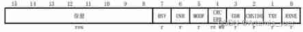
For the receiver , When one frame of data is sent ,“ Status register SR” Medium “TXE Sign a ” Will be placed 1, It means that one frame has been transmitted , Send buffer is empty ; Similarly , When receiving a frame of data ,“RXNE Sign a ” Will be placed 1, It means that one frame has been transmitted , The receive buffer is not empty ; read SPI_DR When the register , Will clear away RXNE position ,SPI The device returns the received data .
SPI Status register (SPI_SR)

 Code :
//SPI1  Read and write a byte
//TxData: Bytes to write
// Return value : Bytes read
uint8_t SPI_FLASH_SendByte(uint8_ TxData)
{
    uint16_t  retry=0;
    while((SPI2->SR&1<<1)==0)       // The waiting area is empty
    {
        retry++;
        if(retry>=0XFFFE)return 0; 	// Timeout exit
    }
    SPI1->DR=TxData;	 	  	    // Send a byte
    retry=0;
    while((SPI2->SR&1<<0)==0)       // Waiting for one to be received byte
    {
        retry++;
        if(retry>=0XFFFE)return 0;	// Timeout exit
    }
    return SPI2->DR;                // Return the received data
}
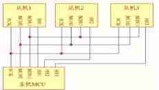
Two 、FLASH control
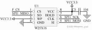
This article uses FLASH And SPI The hardware connection of the bus is shown in the figure below .
Software aspect FLASH Defined very Multiple instructions , Determine the communication protocol module , Send and receive commands through protocol 、 data , Then drive the equipment , Therefore, we need to know the chip timing first , Write drivers by being familiar with the underlying logic , It can also lay a solid foundation for future study . The following are carefully listed as FLASH Read the manufacturer ID Driver implementation steps , See the code list after the text for other drivers .
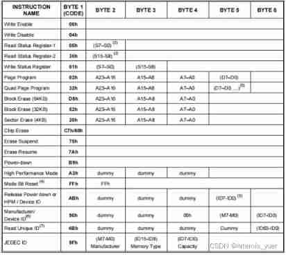
FLASH Instruction set
Read Device ID Sequence diagram

By combining instructions manufacturer ID Required instructions and sequence diagram , Pull down the selection , Can make FLASH, Using user functions SPI_FLASH_SendByte() Come to FLASH Send the first command byte encoding :“W25X_DeviceID”( Custom macros :0xAB); According to the instruction table , After sending this instruction , Followed by three bytes “Dummy byte”, You can customize any value , This is defined as “0xFF”, According to the time sequence , In the 5 Bytes ,FLASH adopt SO The port outputs its device ID, We call functions SPI_FLASH_SendByte() Receive the returned data , And assign it to Temp Variable .SPI_FLASH_ReadDeviceID() The return value of the function is the device obtained by reading ID. Pull up the chip selection signal , End communication . This completes the reading FLASH manufacturer ID.
 Code :

uint32_t SPI_FLASH_ReadDeviceID(void)
{
    uint32_t Temp=0;
    SPI_FLASH_CS_LOW();
    SPI_FLASH_SendByte(W25X_DeviceID);       // Send read instructions
    SPI_FLASH_SendByte(Dummy_Byte);          // Three Dummy_Byte
    SPI_FLASH_SendByte(Dummy_Byte);
    SPI_FLASH_SendByte(Dummy_Byte);
    Temp = SPI_FLASH_SendByte(Dummy_Byte);   // Receive return value
    SPI_FLASH_CS_HIGH();
    return Temp;
}
After compiling and debugging, get manufacturer ID, Compare with the following table , Make sure the chip is selected correctly ,W25Q16 manufacturer ID by 0x14.
Manufacturers and equipment ID

3、 ... and 、 Code writing
main.c
#define FLASH_WriteAddress 0x00000
#define FLASH_ReadAddress FLASH_WriteAddress
#define FLASH_SectorToErase FLASH_WriteAddress
//#define countof(a) (sizeof(a) / sizeof(*(a)))
//#define BufferSize (countof(Tx_Buffer)-1)
#define BufferSize 255
uint8_t Tx_Buffer[255]={0};
//uint8_t Tx_Buffer[] = " A scholar can't do without perseverance , A long way to go \r\n";
uint8_t Rx_Buffer[BufferSize];
int main()
{
uint16_t DeviceID;
uint16_t FlashID;
int cnt=0;
USART1_GPIO_Config();
USART1_Config();
SPI_FLASH_Init();
printf("\r\n This is a 2M Serial flash(W25X16) experiment \r\n");
/* get Flash Device ID */
DeviceID = SPI_FLASH_ReadDeviceID();
DelayMS(200);
/* get Flash ID */
FlashID = SPI_FLASH_ReadID();
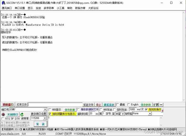
printf("\r\n FlashID is 0x%X, Manufacturer Device ID is 0x%X\r\n", FlashID, DeviceID);
/* erase Flash data */
SPI_FLASH_BulkErase();
SPI_FLASH_SectorErase(0);
printf("\r\n Erase complete \r\n");
/* Write the data of the send buffer to flash in */
SPI_FLASH_Buffer_Write(Tx_Buffer, FLASH_WriteAddress, BufferSize);
{
printf("\r\n The data written is : \r\t");
for(cnt=0;cnt<BufferSize;cnt++)
{
Tx_Buffer [cnt]=cnt;
printf(" 0x%02X ", Tx_Buffer[cnt]);
}
}
//printf("\r\n The data written is :%d \r\t", Tx_Buffer[cnt]);
/* Read out the written data and put it into the receive buffer */
SPI_FLASH_Buffer_Read(Rx_Buffer, FLASH_ReadAddress, BufferSize);
{
printf("\r\n The data read out is : \r\t");
for(cnt=0;cnt<BufferSize;cnt++)
{
Rx_Buffer [cnt]=cnt;
printf(" 0x%02X ", Rx_Buffer[cnt]);
}
}
//printf("\r\n The data read out is :%d \r\n", Rx_Buffer[cnt]);
printf("\r\n 2M Serial flash(W25Q16) Test success !\n\r");
SPI_Flash_PowerDown();
while(1)
{
}
}
spi.c

uint32_t time_out = SPI_FLASH_WAIT_TIMEOUT;
static  uint16_t SPI_TIMEOUT_UserCallback(uint8_t errorCode);

void SPI_FLASH_Init(void)
{
     SPI_InitTypeDef SPI_InitStructure;
     GPIO_InitTypeDef GPIO_InitStructure;

     /*  Can make SPI1  and  GPI The clock  */
     RCC_APB2PeriphClockCmd(RCC_APB2Periph_GPIOA, ENABLE);
     RCC_APB2PeriphClockCmd(RCC_APB2Periph_SPI1, ENABLE);

     /* SCK */
     GPIO_InitStructure.GPIO_Pin = GPIO_Pin_5;
     GPIO_InitStructure.GPIO_Speed = GPIO_Speed_50MHz;
     GPIO_InitStructure.GPIO_Mode = GPIO_Mode_AF_PP;
     GPIO_Init(GPIOA, &GPIO_InitStructure);

     /* MISO */
     GPIO_InitStructure.GPIO_Pin = GPIO_Pin_6;
     GPIO_Init(GPIOA, &GPIO_InitStructure);

     /* MOSI */
     GPIO_InitStructure.GPIO_Pin = GPIO_Pin_7;
     GPIO_Init(GPIOA, &GPIO_InitStructure);

     /* CS */
     GPIO_InitStructure.GPIO_Pin = GPIO_Pin_2;
     GPIO_InitStructure.GPIO_Mode = GPIO_Mode_Out_PP;
     GPIO_Init(GPIOA, &GPIO_InitStructure);

     SPI_FLASH_CS_HIGH();

     /* SPI1 To configure  */
     SPI_InitStructure.SPI_Direction = SPI_Direction_2Lines_FullDuplex;
     SPI_InitStructure.SPI_Mode = SPI_Mode_Master;
     SPI_InitStructure.SPI_DataSize = SPI_DataSize_8b;
     SPI_InitStructure.SPI_CPOL = SPI_CPOL_High;
     SPI_InitStructure.SPI_CPHA = SPI_CPHA_2Edge;
     SPI_InitStructure.SPI_NSS = SPI_NSS_Soft;
     SPI_InitStructure.SPI_BaudRatePrescaler = SPI_BaudRatePrescaler_4;
     SPI_InitStructure.SPI_FirstBit = SPI_FirstBit_MSB;
     SPI_InitStructure.SPI_CRCPolynomial = 7;
     SPI_Init(SPI1, &SPI_InitStructure);

     SPI_Cmd(SPI1, ENABLE);
}


// Send a byte ( The principle here is the same as the previous register code )
 uint8_t SPI_FLASH_SendByte(uint8_t byte)
{
     uint8_t read_temp;
	 time_out = SPI_FLASH_WAIT_TIMEOUT;

     while (SPI_I2S_GetFlagStatus(SPI1, SPI_I2S_FLAG_TXE) == RESET)
	 {
		  if(time_out-- == 0)        // Overtime
		  {
			   return SPI_TIMEOUT_UserCallback(1);
		   }
	  }

    SPI_I2S_SendData(SPI1, byte);
    time_out = SPI_FLASH_WAIT_TIMEOUT;
    /* Wait to receive a byte */
    while (SPI_I2S_GetFlagStatus(SPI1, SPI_I2S_FLAG_RXNE) == RESET)
    {
		  if(time_out-- == 0)
		  {
			   return SPI_TIMEOUT_UserCallback(2);
		  }
	 }
    read_temp = (uint8_t)SPI_I2S_ReceiveData (SPI1);
    return read_temp;
 }


 // Receive a byte
uint8_t SPI_FLASH_Receive_Byte(void)
{
	return SPI_FLASH_SendByte(0xFF);
}


 // Call this function when there is an error
static  uint16_t SPI_TIMEOUT_UserCallback(uint8_t errorCode)
{
	printf("\r\nSPI  Detection timeout , Error code :%d",errorCode);
	return 0;
}
flash.h
#ifndef __FLASH_H
#define __FLASH_H

#include "sys.h"

#define W25Q16 	0XEF14
#define FLASH_ID 0XEF14

#define	SPI_FLASH_CS PAout(2)
#define SPI_FLASH_CS_HIGH()  GPIO_SetBits(GPIOA, GPIO_Pin_2)
#define SPI_FLASH_CS_LOW()    GPIO_ResetBits(GPIOA, GPIO_Pin_2)
#define SPI_FLASH_PageSize         256
#define SPI_FLASH_PerWritePageSize  256
#define  SPI_FLASH_WAIT_TIMEOUT  10000

// Instruction list
#define W25X_WriteEnable		0x06
#define W25X_WriteDisable		0x04
#define W25X_ReadStatusReg		0x05
#define W25X_WriteStatusReg		0x01
#define W25X_ReadData			0x03
#define W25X_FastReadData		0x0B
#define W25X_FastReadDual		0x3B
#define W25X_PageProgram		0x02
#define W25X_BlockErase			0xD8
#define W25X_SectorErase		0x20
#define W25X_ChipErase			0xC7
#define W25X_PowerDown			0xB9
#define W25X_ReleasePowerDown	0xAB
#define W25X_DeviceID			0xAB
#define W25X_ManufactDeviceID	0x90
#define W25X_JedecDeviceID		0x9F

#define Dummy_Byte 0xFF

uint32_t SPI_FLASH_ReadDeviceID(void);
uint8_t SPI_FLASH_SendByte(uint8_t byte);
uint8_t SPI_FLASH_Receive_Byte(void);
uint32_t SPI_FLASH_ReadID(void);
void SPI_FLASH_SectorErase(uint32_t SectorAddr);
void SPI_FLASH_BulkErase(void);
void SPI_FLASH_WriteEnable(void);
void SPI_FLASH_WaitForWriteEnd(void);
void SPI_FLASH_Page_Write(uint8_t* pBuffer, uint32_t WriteAddr, uint16_t NumByteToWrite);
void SPI_FLASH_Buffer_Read(uint8_t* pBuffer, uint8_t ReadAddr, uint8_t NumByteToRead);
void SPI_FLASH_Buffer_Write(uint8_t* pBuffer, uint32_t WriteAddr, uint16_t NumByteToWrite);
void SPI_Flash_PowerDown(void);

#endif   /* __FLASH_H */
usart.c
void USART1_GPIO_Config()                                                /* GPIO To configure  */
{
    GPIO_InitTypeDef GPIO_InitStruct;                                    /*  Structure definition  */

	RCC_APB2PeriphClockCmd(RCC_APB2Periph_USART1, ENABLE);               /* USART1 The clock  */
    RCC_APB2PeriphClockCmd(RCC_APB2Periph_GPIOA, ENABLE);                /* GPIOA Can make  */
    GPIO_InitStruct.GPIO_Pin=GPIO_Pin_9;                                 /* PA2 Pin  ,USART Of TX*/
    GPIO_InitStruct.GPIO_Mode=GPIO_Mode_AF_PP;                           /*  Multiplexing push pull output  */
    GPIO_InitStruct.GPIO_Speed=GPIO_Speed_50MHz;                         /* 50MHz*/
    GPIO_Init(GPIOA,&GPIO_InitStruct);                                   /*  initialization GPIOA */
	GPIO_InitStruct.GPIO_Pin=GPIO_Pin_10;                                /* PA3 Pin  ,USART Of RX*/
    GPIO_InitStruct.GPIO_Mode=GPIO_Mode_IN_FLOATING;                     /*  Floating input , Used to receive data  */
	GPIO_Init(GPIOA,&GPIO_InitStruct);                                   /*  initialization GPIOA */
}

void USART1_Config()
{
    USART_InitTypeDef USART_InitStructure;                                 /*  Structure definition  */

    USART_InitStructure.USART_BaudRate = 115200;                           /*  Configure baud rate  */
    USART_InitStructure.USART_WordLength = USART_WordLength_8b;            /* 8 Bit data  */
    USART_InitStructure.USART_StopBits = USART_StopBits_1;                 /* 1 Bit stop bit  */
    USART_InitStructure.USART_Parity = USART_Parity_No ;                   /*  No parity  */
    USART_InitStructure.USART_HardwareFlowControl = USART_HardwareFlowControl_None;/*  No hardware flow control  */
    USART_InitStructure.USART_Mode = USART_Mode_Rx | USART_Mode_Tx;        /*  Allow receiving and sending  */

    USART_Init(USART1, &USART_InitStructure);                              /*  Complete serial port initialization  */

    USART_Cmd(USART1, ENABLE);                                             /*  Serial port enable  */

}


// redefinition printf function
int fputc(int ch, FILE *f)
{
    /*  take Printf Send the content to the serial port  */
    USART_SendData(USART1, (unsigned char)ch);
    while (!USART_GetFlagStatus(USART1, USART_FLAG_TC));
    USART_ClearFlag(USART1, USART_FLAG_TC);
    return (ch);

}


int fgetc(FILE *f)
{
    /*  Wait for serial port input data  */
    while (USART_GetFlagStatus(USART1, USART_FLAG_RXNE) == RESET);
    return (int)USART_ReceiveData(USART1);
}
Four 、 Running results
After compiling and debugging , The running results of using serial port monitoring are as follows :

5、 ... and 、 Conclusion
When SPI When the clock frequency is high , The proposal USES DMA Mode to avoid SPI Reduction of speed performance , And SPI There is a drawback : There is a specified flow control , There is no response mechanism to confirm whether data has been received , Unlike I2C There will be one without transmitting data ACK Response mechanism , It is particularly important to learn timing and clarify the underlying logic , Don't muddle along .
边栏推荐
- 如何实现实时音视频聊天功能
- American 5g open ran suffered another major setback, and its attempt to counter China's 5g technology has failed
- What is test development? Why do so many companies hire test developers now?
- 在线SQL转Excel(xls/xlsx)工具
- NetSetMan pro (IP fast switching tool) official Chinese version v5.1.0 | computer IP switching software download
- 学习MVVM笔记(一)
- MindFusion. Virtual Keyboard for WPF
- [phantom engine UE] only six steps are needed to realize the deployment of ue5 pixel stream and avoid detours! (the principles of 4.26 and 4.27 are similar)
- Threejs realizes rain, snow, overcast, sunny, flame
- 3. Package the bottom navigation tabbar
猜你喜欢
EasyCVR更改录像存储路径,不生成录像文件如何解决?
CTF stegano practice stegano 9

Enterprise level: spire Office for . NET:Platinum|7.7. x

UI automation test farewell to manual download of browser driver
Containerd series - detailed explanation of plugins
Threejs Internet of things, 3D visualization of farms (I)
Laravel8 export excel file

A real day for Beijing programmers!!!!!

Special Edition: spreadjs v15.1 vs spreadjs v15.0
Online sql to excel (xls/xlsx) tool
随机推荐
[charging station]_ Secular wisdom_ Philosophical wisdom _
IronXL for . NET 2022.6
How to realize real-time audio and video chat function
Serpentine matrix
学习MVVM笔记(一)
[Chongqing Guangdong education] 2408t Chinese contemporary literature reference test in autumn 2018 of the National Open University
provide/inject
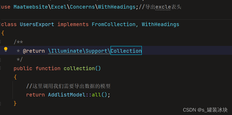
laravel8 导出Excle文件
Rome链分析
DFS and BFS concepts of trees and graphs
为什么百度、阿里这些大厂宁愿花25K招聘应届生,也不愿涨薪5K留住老员工?
Pyqt5 displays file names and pictures
长度为n的入栈顺序的可能出栈顺序
【虚幻引擎UE】运行和启动的区别,常见问题分析
Rome chain analysis
Uni app change the default component style
10种寻址方式之间的区别
[phantom engine UE] realize the animation production of mapping tripod deployment
[understand series after reading] 6000 words teach you to realize interface automation from 0 to 1
UI automation test farewell to manual download of browser driver