当前位置:网站首页>Kuntai ch7511b scheme design | ch7511b design EDP to LVDS data | pin to pin replaces ch7511b circuit design
Kuntai ch7511b scheme design | ch7511b design EDP to LVDS data | pin to pin replaces ch7511b circuit design
2022-07-08 01:10:00 【qq1659747718】
Quintiles CH7511B The project design |CH7511B Design EDP turn LVDS Information |pin to pin replace CH7511B Circuit design
Chrontel Of CH7511B It's a low cost 、 Low power semiconductor devices , It will be embedded DisplayPort The signal is converted to LVDS( Low pressure differential signal ). This innovative DisplayPort The receiver has an integrated circuit LVDS Transmitter , Designed for multi-functional integration PC And laptop market . adopt CH7511B Advanced decoding / Coding algorithm , Input eDP High speed serial video data can be seamlessly converted into LVDS,LVDS It is a popular Chinese / large LCD Display high-speed serial link display technology . utilize eDP Unique source / Remit “ Link training ” Program , When CH7511B When the initialization process between and the graphics chip is completed ,CH7511B Can immediately report to LCD Show video .CH7511B The design conforms to the embedded system DisplayPort standard 1.2 edition . In the receiving module of the device , It supports two eDP Main link input , Data rate is 1.62Gb/s or 2.7Gb/s, Acceptable 18 position 6:6:6 or 24 position 8:8:8 Of RGB Digital format , For up to 1920x1200 Of LVDS Output . In order to meet GPU New energy-saving plan , For example, reduce the display frame rate ,CH7511B Equipped with dynamic refresh rate switching method , It can be automatically lowered to LVDS The low refresh rate supported by the panel . Integrate LVDS The transmitter supports single port and dual port LVDS Output , To drive up to WUXGA(1920x1200) The display resolution of .CH7511B Supported by GPIO[0:3] The pin controls or writes to the chip register to select the panel . In order to reduce the EMI launch ,CH7511B Of LVDS The encoder block adopts spread spectrum control , Its spread spectrum percentage can be adjusted through internal registers .
CH7511B Parameter properties :
Support embedded DisplayPort(eDP) standard 1.2 edition .
Support 2 The main chain , The link rate is 1.62Gb/s or 2.7Gb/s, Suitable for laptop applications
Support to input color depth 6, Each pixel 8 Bit RGB Format
Support enhanced frame mode
Support VESA and CEA Timing standard , Resolution up to 1920x1200,8 An input , The refresh rate is 60Hz
Support dynamic refresh rate switching
Support Gamma correction
Panel tuning methods include jitter and 6 position +FRC
The embedded DisplayPort Fast full link training of the system
Support eDP authentication : Optional scrambling seed reset and optional framing
2 Working mode : Connect 27MHz Crystal , Inject 27MHz The clock
Programmable LCD panel power sequence
Support 18 Bit single port 、18 Bit dual port 、24 Bit single port and 24 Bit dual port LVDS Output interface
Support LVDS Application's OpenLDI and SPWG Bit mapping
Support panel selection by GPIO The pin controls or writes to the chip register .
agile LVDS Output pin exchange
Blank panel when invalid input
Support PWM. The backlight brightness is controlled through the auxiliary channel ,PWM Pins and BLUP/BLDN The pin supports dynamic backlight control
BLUP/BLDN Support when the pin controls the backlight brightness OSD Show
Hot swap detection
Boot is loaded automatically when starting up ROM
Serial boot ROM Data is passed through I2C Bus or auxiliary channel update
Programmable power management
eDP Input and LVDS Output EMI Reduce capacity . Spread spectrum control can be used for transmission LVDS The signal
QFN68 encapsulation
CH7511B Package pin :

CH7511B Design EP turn LVDS Block diagram of scheme structure :

Capstone The new CS5211 It can be completely compatible and replace CH7511.CS5211 It's a eDP To LVDS converter , Flexible configuration , Suitable for low cost display system .CS5211 And eDP 1.2 compatible , Support 1 Channels and 2 Channel mode , The speed of each channel is 1.62Gbps and 2.7Gbps.CS5211 Use powerful SerDes Technology
Technique , It can recover high speed serial data with low bit error rate .CS5211 LVDS The transmitter supports single port and dual port modes .CS5211 The maximum resolution supported is WUXGA(1920x1200).CS5211 Yes 4 Configuration pins , Can support 16 A different combination EEPROM Panel resolution and resolution of the image LVDS Working mode . Besides ,
It also provides a simple tool to edit 、 Generate and update EEPROM Images for custom configuration . By optimizing the design , Use CS5211 It's good for saving BoM cost . The chip integrated clock source , The external crystal is saved , Support a wide range of power supply ( The core power is 1.8~1.2V), Save on-board power equipment ,CS5211 The total power of is less than
300mW, Simplify the design of power supply network . It's easy to put CS5211 Integrated into popular low cost display systems .
CS5211 The parameter characteristics are as follows :

边栏推荐
猜你喜欢
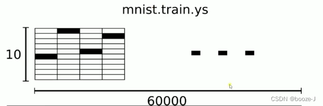
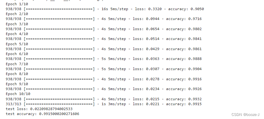
3. MNIST dataset classification
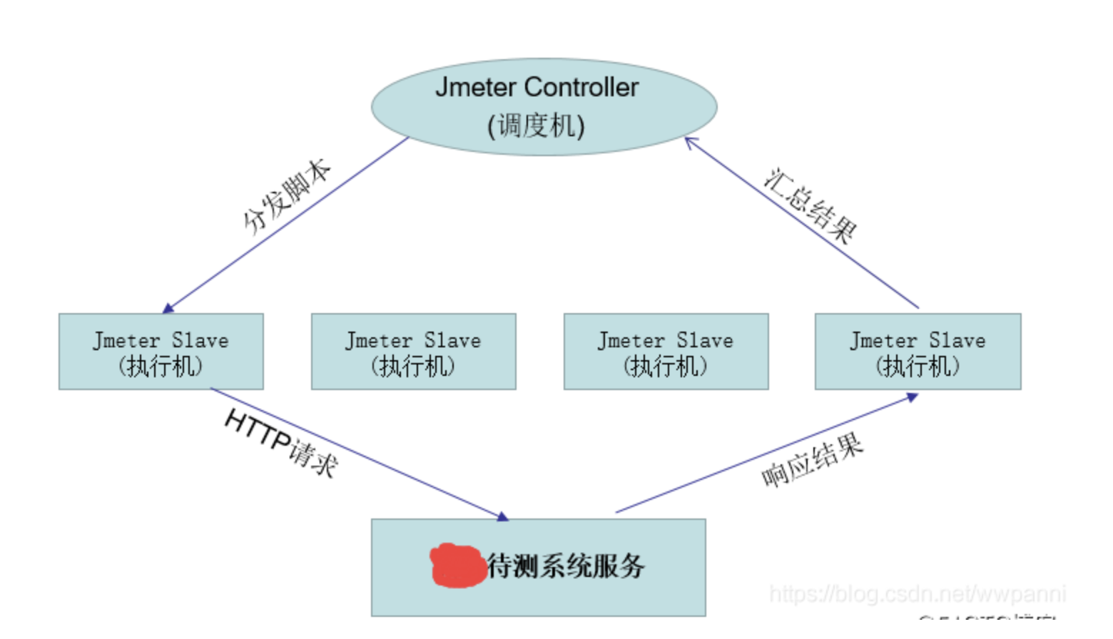
Jemter distributed
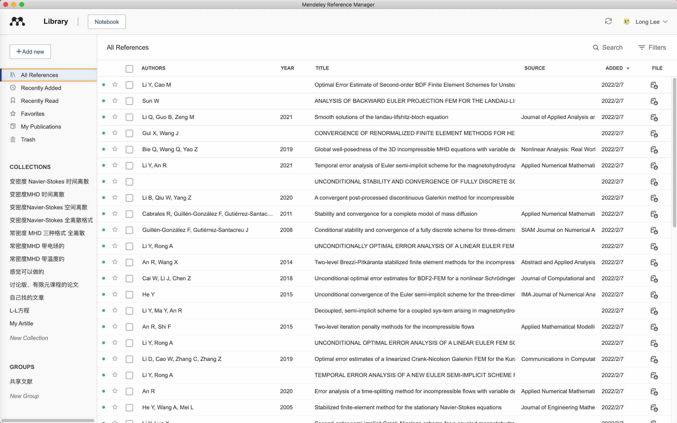
Recommend a document management tool mendely Reference Manager
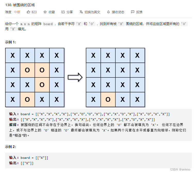
130. 被圍繞的區域
10. CNN applied to handwritten digit recognition
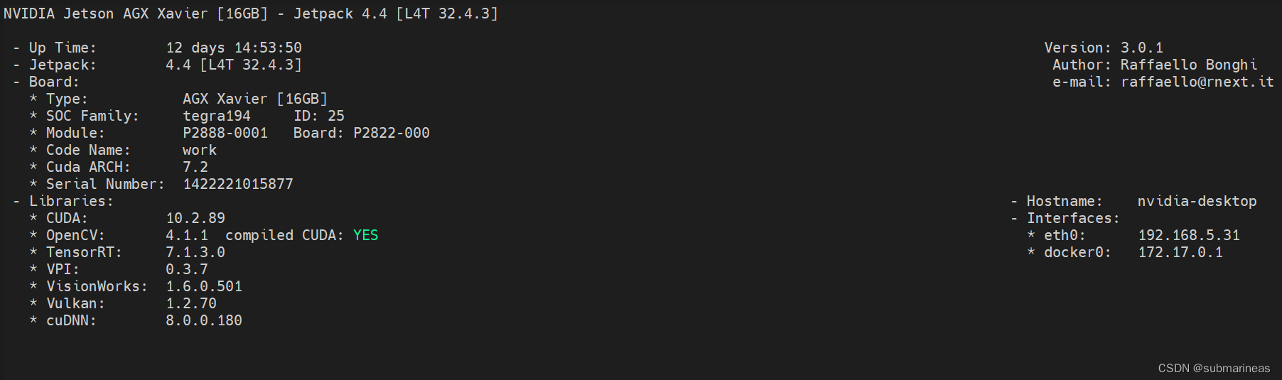
NVIDIA Jetson test installation yolox process record
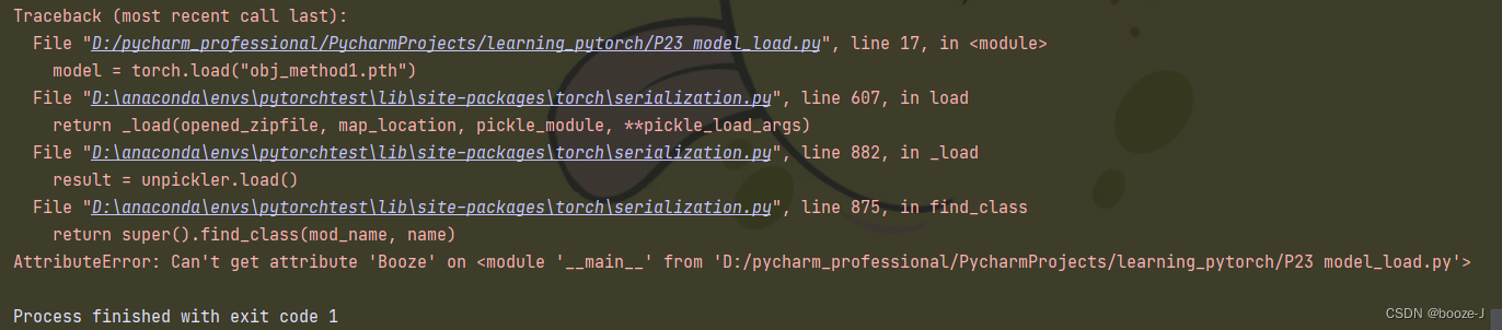
Saving and reading of network model
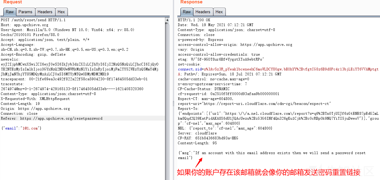
Password recovery vulnerability of foreign public testing
11.递归神经网络RNN

Cancel the down arrow of the default style of select and set the default word of select
随机推荐
130. Surrounding area
Su embedded training - Day7
Ag9310 for type-C docking station scheme circuit design method | ag9310 for type-C audio and video converter scheme circuit design reference
A speed Limited large file transmission tool for every major network disk
Malware detection method based on convolutional neural network
Codeforces Round #804 (Div. 2)(A~D)
Chapter 7 Bayesian classifier
Analysis of 8 classic C language pointer written test questions
Y59. Chapter III kubernetes from entry to proficiency - continuous integration and deployment (III, II)
Recommend a document management tool mendely Reference Manager
German prime minister says Ukraine will not receive "NATO style" security guarantee
STL -- common function replication of string class
[Yugong series] go teaching course 006 in July 2022 - automatic derivation of types and input and output
Ag9310meq ag9310mfq angle two USB type C to HDMI audio and video data conversion function chips parameter difference and design circuit reference
Stock account opening is free of charge. Is it safe to open an account on your mobile phone
9.卷积神经网络介绍
Su embedded training - C language programming practice (implementation of address book)
Basic mode of service mesh
Complete model verification (test, demo) routine
Cascade-LSTM: A Tree-Structured Neural Classifier for Detecting Misinformation Cascades(KDD20)