当前位置:网站首页>A hodgepodge of ICER knowledge points (attached with a large number of topics, which are constantly being updated)
A hodgepodge of ICER knowledge points (attached with a large number of topics, which are constantly being updated)
2022-07-07 18:58:00 【Eight four one one】
Catalog
- 1.IC Basics
- 1.1 Latch trigger structure
- 1.2 Establish hold time
- 1.3 STA
- 1.4 CDC
- 1.5 How to solve metastable state
- 1.6 Low power common design
- 1.7 Competition and adventure
- 1.8 skin needling
- 1.9 IC Design process
- 1.10 Complement code 、 Original code 、 Inverse code
- 1.11 Gray code 、 Hot code alone
- 1.12 fifo depth
- 1.13 Binary decimal conversion
- 1.14 Operator priority
- 2. Code of hand tear
- 2.1 asynchronous fifo
- 2.2 Sync fifo
- 2.3 A divider
- 2.4 Multiplier
- 2.5 Carry ahead adder
- 2.6 Edge monitor
- 2.7 Input anti shake
- 2.8 Deburring
- 2.9 Counter
- 2.10 Burr free switching
- 2.11 shift register
- 2.12 Odd frequency division
- 2.13 Even frequency division
- 2.14 Sequence check
- 2.15 Pulse broadening
- 2.16 Two series asynchronous reset T trigger
- 2.17 For the input 32 Bit data for parity , according to sel Output verification results (0 Output odd check ,1 Output parity )
- 3. Circuit knowledge
- 4. Brush, brush
1.IC Basics
1.1 Latch trigger structure
① Latch 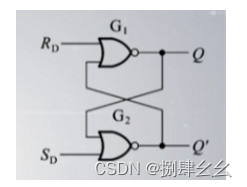
We define :
①Q = 1, And Q’ = 0 For latches 1 state
②Q = 0, And Q’ = 1 For latches 0 state
③Q For the current state ,Q* For the next state ,Q’ by Q back
Its truth table and functions are as follows :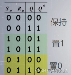
② trigger 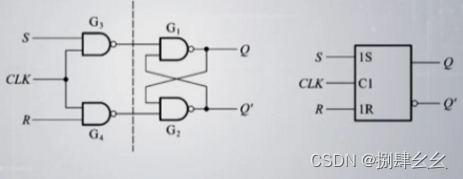
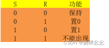
The difference between a trigger and a latch is , It can only be set 1 Set up 0 Outside the input end , Another trigger signal input is added , Only when the trigger signal comes , The trigger can be set according to the input 1、 Set up 0 The signal is set to the corresponding state , And keep it going , We call this trigger signal clock signal , Write it down as CLK.
Here are several types of triggers :
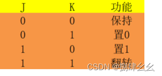
SR trigger :Q* = S + R’Q
JK trigger :Q* = JQ’ + K’Q
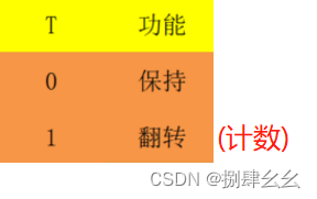
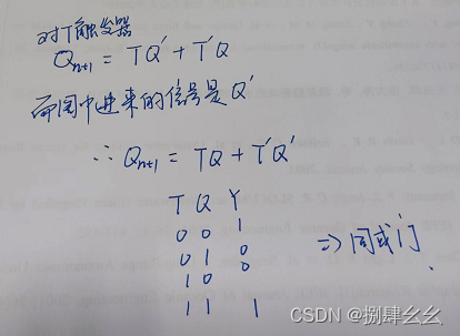
T trigger :Q* = TQ’ + T’Q
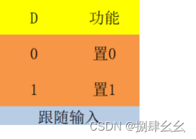
D trigger :Q* = D
1.2 Establish hold time
1.3 STA
1.4 CDC
1.5 How to solve metastable state
1.6 Low power common design
1.7 Competition and adventure
1.8 skin needling
1.9 IC Design process
1.10 Complement code 、 Original code 、 Inverse code
1.11 Gray code 、 Hot code alone
1.12 fifo depth
1.13 Binary decimal conversion
- 10 Hexadecimal number 101.25, Convert to 2 The binary number is ?
101 There is no need to say more about converting to binary , Short division , Reading degrees from bottom to top , Look at the picture below : The non decimal part is 1100101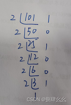
The decimal part is x2 Rounding processing , Then the decimal part continues x2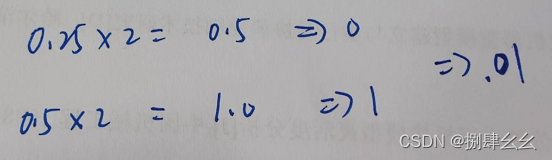
So the answer is 1100101.01
- The above question is reversed ? How to convert binary decimal into 10 Base number ?
-1 Power 、-2 The form of power
Such as :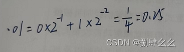
1.14 Operator priority
2. Code of hand tear
2.1 asynchronous fifo
2.2 Sync fifo
2.3 A divider
2.4 Multiplier
2.5 Carry ahead adder
2.6 Edge monitor
2.7 Input anti shake
2.8 Deburring
2.9 Counter
2.10 Burr free switching
2.11 shift register
2.12 Odd frequency division
2.13 Even frequency division
2.14 Sequence check
Design a sequence detector , Transfer the data in the code stream “10010” Sequence detected :
① Three inputs ,clk,rst_n,x, among x It is the input of a person , from x A plurality of transmitted data constitute a code stream
② Output z, Complete... Is detected 10010 In sequence ,z pull up
The method of using shift register is much simpler than the method code of state machine , Let's talk about the principle first :
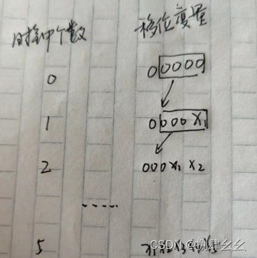
- So let's define one 5 Bit variables are used to shift ——shift = 5’b00000;
- Then enter each digit x, Shift to shift in ——shift <= {shift[3:0], x};
module check_num_shift
(
	input		clk,
	input		rst_n,
	input		x,
	output wire	z
);

reg [4:0]	shift;

[email protected](posedge clk or negedge rst_n)begin
	if(!rst_n)
		shift <= 0;
	else
		shift <= {
    shift[3:0],x};
end

assign z = (shift == 5'b10010)?1:0;

endmodule
2.15 Pulse broadening
Yes 1bit The pulse signal of , To 32bit A wide , And generate effective signals
- First of all, what does the title mean ? That is to say, here you are 1T Pulse signal with cycle width , I want you to make 32T Width , And take effective signal output
- Ideas : The edge monitor identifies the falling edge of the pulse , Output valid signal ; Use a counter to set 1T Delay to 32T
- Code :
module 1_to_32(
    input           clk,
    input           rst_n,
    input           pulse_in,
    output reg      pulse_out,
    output wire     flag
);
//-------------------------------------------------------
reg pulse_in_ff0,pulse_in_ff1;
reg [4:0]   cnt;
//-------------------------------------------------------
// Jianyan ( Falling edge )
always @(posedge clk or negedge rst_n)begin
    if(!rst_n) begin
        pulse_in_ff0<=1'b0;
        pulse_in_ff1<=1'b0;
    end
    else begin
        pulse_in_ff0 <= pulse_in;
        pulse_in_ff1 <= pulse_in_ff0;
    end
end
// The previous shot is 0, For now 1, Is the rising edge
assign  flag=(~pulse_in_ff1)&pulse_in_ff0;
//-------------------------------------------------------
// Count extended 32 A clock
always @(posedge clk or negedge rst_n)begin
    if(!rst_n)
        pulse_out<=1'b0;
    else if(flag)
        pulse_out<=1'b1;
    else if(cnt==5'd31)
            pulse_out<=1'b0;
end

 always @(posedge clk or negedge rst_n)begin
    if(!rst_n)
        cnt<=5'b0;
    else if(pulse_out==1'b1)begin
        	if(cnt==5'd31)
            cnt<=5'd0;
        	else
            cnt<=cnt+1'b1;
        end
end
//-------------------------------------------------------

endmodule
2.16 Two series asynchronous reset T trigger
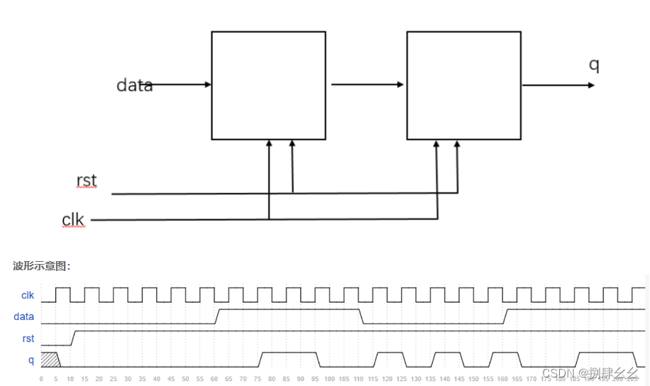
- T The formula of trigger is Q* = TQ’ + T’Q , Equivalent to an XOR operation
- So two levels tff that will do
`timescale 1ns/1ns
module Tff_2 (
input wire data, clk, rst,
output wire q
);
//*************code***********//
    reg data_tff0;
    reg data_tff1;

    [email protected](posedge clk or negedge rst)begin
        if(!rst)begin
            data_tff0 <= 0;
            data_tff1 <= 0;
        end
        else begin
            data_tff0 <= data^data_tff0;
            data_tff1 <= data_tff0^data_tff1;
        end
    end

    assign q = data_tff1;

//*************code***********//
endmodule
2.17 For the input 32 Bit data for parity , according to sel Output verification results (0 Output odd check ,1 Output parity )
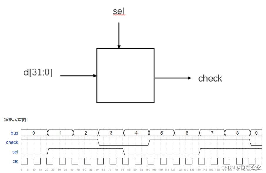
- First of all, you should understand the principle of parity : Add a check bit to the code to make it 1 The number of is odd or even
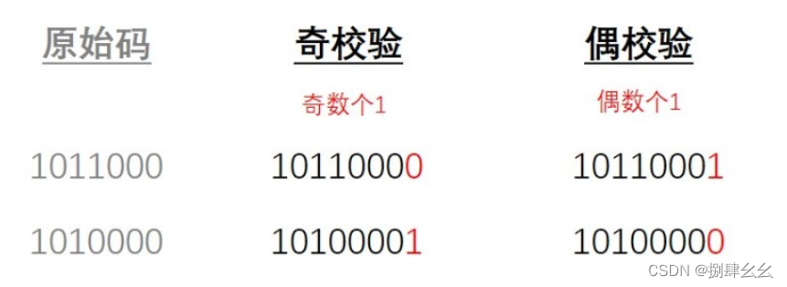
- So how do we find parity bits ? The answer is XOR
Take a chestnut , stream 101 , The odd parity bit is 1, The parity bit is 0 , The result of data direct XOR is 0, It happens to be even check , Then the odd check is reversed - The code is as follows :
`timescale 1ns/1ns
module odd_sel(
input [31:0] bus,
input sel,
output check
);
//*************code***********//
    wire ji;
    wire ou;
    wire check;

    assign ou = ^bus;
    assign ji = ~ou;
    assign check = (sel) ? ou :ji;

//*************code***********//
endmodule
3. Circuit knowledge
3.1 Min max term and Karnaugh map
N Expression of product terms ( And item ), Such as two variables AB The minimum term of is A’B’、A’B,、AB’、AB
  The properties of the minimum term :
 		① Under any value of the input variable , The value with and only one minimum term is 1;
 		② The sum of all minimum terms is 1 ;
 		③ The product of any two minimum terms is 0 ;
 		④ The sum of two adjacent minimum terms can be combined , Eliminate a pair of factors , Leave only the common factor ;( The important principle of Karnaugh map )
 		 adjacent : The smallest term with only one factor different , Such as :A'BC' And A'BC;
N Expression of items and ( Or item ), Such as two variables AB The maximum term of is A’+B’、A’+B,、A+B’、A+B
  The properties of the largest term :
 		① Under any value of the input variable , The value of having and only one maximum item is 0 ;
 		② The product of all the largest terms is 0 ;
 		③ The sum of any two largest terms is 1 ;
 		④ The product of two adjacent largest terms can be merged , Eliminate a pair of factors , Leave only the common factor .
 		 adjacent : There is only one maximum term with different factors , Such as :A'+B+C and A'+B+C
Karnaugh map : For simplification
 ① Turn the function into the form of the sum of the minimum terms
 ② Draw a Karnaugh map (00、01、11、10  Gray code ), Fill in the smallest item 1
 ③ Circle it !
  circle 1 principle :
  Cover all 1
  The number of circles should be minimized
  Inside the circle 1 As much as possible
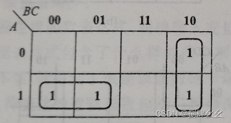
Pictured above , Find a public item
The horizontal circle is AB’
The vertical circle is BC’
The result is AB’ + BC’
3.2 MOS Tube principle
Generally speaking : stay DS Apply voltage at both poles ,DS No conduction ; stay GS Apply voltage ,DS Forming channels between makes DS Conduction 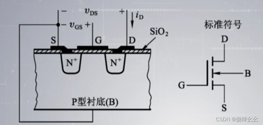
It can also be divided into three areas :
① When Vgs < Vgs(th) when , That is, when it is less than the starting voltage , This part of the area becomes the cut-off area
② When Vgs > Vgs(th) when , As shown in the figure above , The left side of the dotted line becomes the variable resistance area , Its equivalent resistance is the same as Vgs of
③ To the right of the dotted line is the constant current area , At this time, the current is basically from Vgs decision 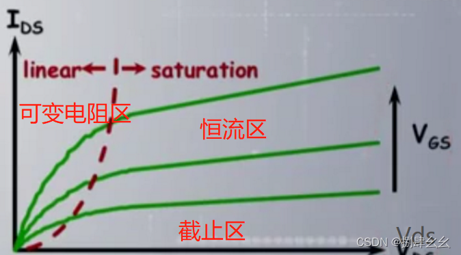
3.3 TTL Tube principle
① Cut off zone : Conditions Vbe= 0, ib = 0, ic = 0, c One e between “ To break off ”
② Zoom in : Conditions Vce> 0.7, ib>0, ic along with ib Change in direct proportion , △ic=β△ib
③ Saturation zone : Conditions Vce< 0.7, ib >0, Vce Very low ,△ic along with △ib Increase and slow down , Tend to “ saturated ”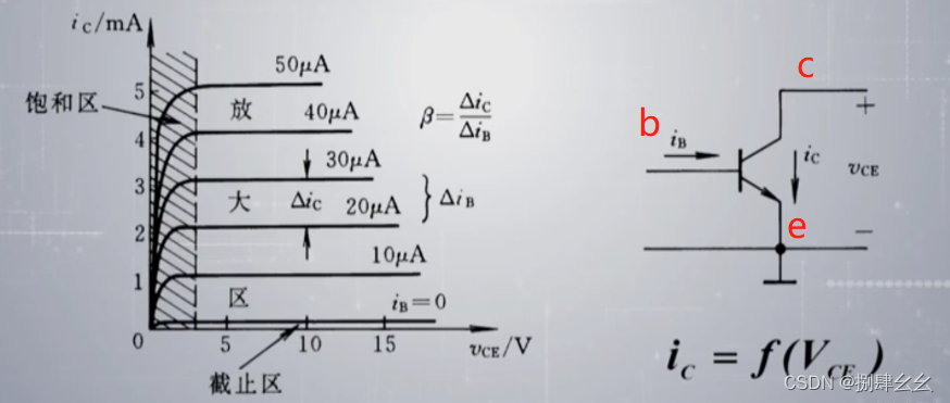
3.4 Trigger type
front 1.1 It's been said , It's not about
3.5 Multivibrator circuit
- Multivibrator circuit is a self-excited oscillation circuit
- After the power is turned on , No additional trigger signal is required , It can automatically generate rectangular pulses
- Because the rectangular wave contains rich high-order harmonic components , Conventionally, rectangular wave oscillation circuit is also called multiharmonic oscillation circuit
① Symmetrical multivibrator : A positive feedback oscillation circuit with two inverters coupled with two capacitors .
② Asymmetric multivibrator : Simplify on the basis of symmetry .
③ Schmidt multivibrator : The inverting output of Schmidt trigger circuit is used RC The integral is connected back to the input .
④ Ring oscillator : Oscillation is generated by delayed negative feedback .
⑤ Quartz crystal multivibrator : Quartz crystal + Symmetrical ( Connect quartz crystal to stabilize frequency )
3.6 Monostable circuit
The operating characteristics of monostable circuits have the following remarkable characteristics :
- First of all , It has two different working states: steady state and transient steady state
- second , Under the action of external trigger pulse , Can flip from steady state to transient state , After the transient state is maintained for a period of time , Then automatically return to the steady state
- Third , The duration of transient steady state depends on the parameters of the circuit itself , Independent of the wide amplitude of the trigger pulse
Example : acoustic control lamp , When it goes out, it is steady 、 The light is transient
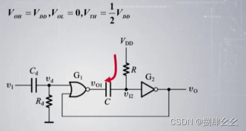
principle :
① When vi = 0,vi2 = vdd, therefore vo = 0
② When vi When pulse is connected , stay cd and rd Narrow pulses will be generated between vd, When vd = vth after , The following positive feedback occurs 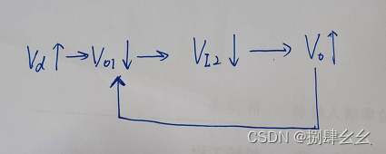
③ Quickly make vo1 = vi2 = 0
④ Because the capacitor voltage will not jump rapidly , Therefore, it enters the transient state
⑤ When vdd After charging the capacitor , Enter steady state again
- There are two types of monostable circuits :
① Differential type : It can be triggered by narrow pulses 、 The falling edge of the output pulse is poor
② Integral type : Strong anti-interference ability 、 The output edge is poor
3.7 Schmidt trigger circuit
① The input signal is rising and falling , The input level of circuit state transition is different
② There is a positive feedback process when the circuit state changes , Steepen the edge of the output waveform
③ For waveform transformation
④ For amplitude monitoring
⑤ For pulse shaping 
principle :
① When vi = 0 ,vo = vol = 0 , This is a va It's also 0
② and vi from 0 Rise to vth,CMOS tube G1 Conduction , Cause the following positive feedback 
③ here vo Quickly rise to vdd, And then vi The value of is what we call vt+
④ Empathy vi from vdd Down to vt-,vo from voh become vol, It is also a positive feedback process
3.8 Logical computing
A watch is enough 
3.9 Line and
- Line and, to put it bluntly, are physically connected 、 Select the connection on the appliance
- Line and in ttl There are two in the tube OC NAND gate ( Open collector gate ) To achieve
- Line and in mos There are two in the tube OD NAND gate ( Open drain gate ) To achieve
- Their rough pictures are as follows , Only when Y1Y2 All are 1,Y Just output 1
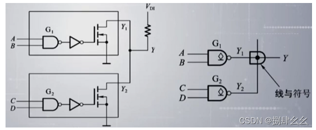
So why do I need to use OD/OC Door to do line with it ? You can see OD The characteristics of the door :
① The driving ability of external circuits can be used , Reduce IC Internal drive , Or drive a load with a higher power voltage than the chip
② Multiple open drain outputs can be Pin, Connect to a line , This is the occupation principle of some buses
③ It can be used to change the voltage of the pull-up power supply , Change transmission level ; If you add a pull-up resistor, you can provide TTL/CMOS Level output
④ natural CMOS The output stage is up 、 The next two tubes , Take out the upper pipe OPEN-DRAIN(OD)
⑤ shortcoming :OD The door provides a flexible output mode , But it also brings the delay of rising edge
4. Brush, brush
1 Transistors are used for amplification , Work in what area ?
Zoom in ( Also called linear region ) : Conditions Vce> 0.7, ib>0, ic along with ib Change in direct proportion , △ic=β△ib
0.7 Of Von It's a silicon triode , Germanium triode is 0.3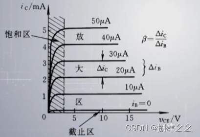
2CMOS The tube is used for switching , Work in what area ?
Single MOS Tube time , Look at the picture below ;
The input is low power level ,MOS The tube is in the cut-off zone , Output high level 1;
The input is high power level ,MOS The pipe is open ( I feel that I work in the variable resistance area ), Output low level 0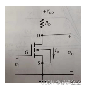
When it comes to CMOS Tube time , Look at the picture below ;
Whether the input is high level or low level , Two MOS Tubes are always connected one by one , That is the so-called complementary relationship ;
and CMOS Medium C It means complementary ;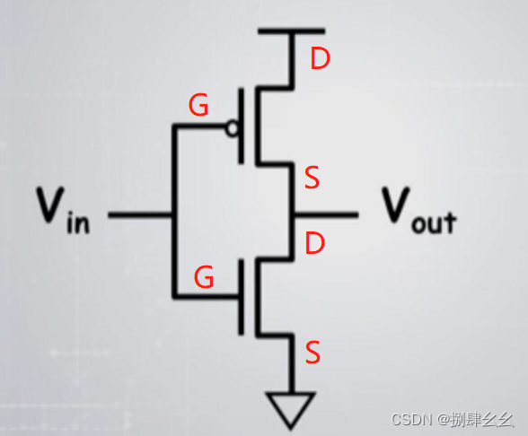
3 Design a sequence generator , With CLK Is the control signal , The output sequence is 0010110111
module check_num_shift
(
	input		clk,
	input		x,
	output wire	is_it
);

reg [9:0]	shift;

[email protected](posedge clk)begin
		shift <= {
    shift[8:0],x};
end
assign is_it= (shift == 10'b0010110111)?1:0;

endmodule
4 Gongyang nixie tube ( Such as graphic ) Display decoder , When the input A3A2A1A0 by 0101 when , What is the output
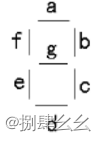
Input is 0101 That is to display numbers 5, therefore afgcd Light up , Set up 0, Other settings 1 , So the output is 0100100
5.5 With counting function T Trigger link , The input pulse frequency is 256KHZ, Then what is the output pulse frequency of the highest trigger of this counter
Each input clock pulse , The trigger state is reversed once , Realize primary frequency division , therefore 5 One is divided by 2^5, Finally 8KHZ
6 What is? BCD Code counter ? stay 4 Triggers 8421BCD Code counter , Has several unrelated States ?
BCD Code is used 4 Bit binary number to represent 1 In decimal digits 0~9 this 10 Number , therefore BCD The code counter is 0-9 The counter of ,4 Bit triggers share 16 States , So there's more 6 An unrelated state
7 If the output resolution of the sensor is 1mV,ADC The power supply for 5V, The reference voltage is 2.5V, To guarantee ADC The sampling accuracy of ,ADC What is the number of digits at least ?
The output voltage of the sensor is an analog signal , It is used as a ADC The input signal of , Its resolution is 1mV, To guarantee ADC Sampling accuracy ,n position ADC The smallest analog voltage that can be distinguished is 1mV; The formula of resolution is as follows ,Vref Is the reference voltage 2.5
So it's calculated n The minimum is 12 position
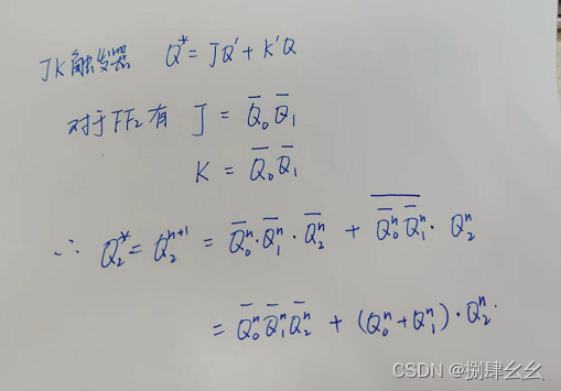
8 Analyze the circuit shown in the figure below , Set the initial state of each trigger as 0, Work out Q2n+1 The equation of 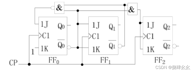
9 When measuring the current of high-voltage circuit , Which end should the ammeter be connected to ?
At the zero potential end , The common mode voltage borne by the ammeter is small .
10 For an asynchronous fifo, List all the test points you can think of ?
It's not a problem to list the signals one by one
- Write port timing behavior is consistent with the description , Check the data in wr The sampled time is correctly written
- The timing behavior of the read port is consistent with the description , Check the data in rd Read out correctly at the sampling time
- Empty signals can be generated correctly
- Full signal can be generated correctly
- Whether there is read-write protection to prevent data coverage after writing full and reading empty
- Whether there is read-write protection to prevent the empty and full signal from being disordered after writing full and reading empty
- Whether it can be reset normally , Initial state of each output signal after reset ( reset value ) If there is something wrong
- Correctness of gray code conversion logic
11 Use only (2 choose 1MUX) Complete XOR gate logic , At least how many MUX
Y = A’B +AB’, namely :A=0 when ,Y = B;A=1 when ,F = Y’
12 The timing analysis of asynchronous reset circuit in timing check is ?
- recovery time: recovery time
When canceling reset , The level to be restored to the de reset state must come some time before the effective edge of the clock comes , To ensure that the clock can be effectively restored to the de reset state , This period is recovery time.
- removal time : Removal time
Reset time , After the effective edge of the clock comes, the time that the reset signal still needs to be maintained is the removal time removal time
13 The correct description of Yu netlist simulation is ?
A. Netlist simulation cannot find the problem of implementing constraints
B. Simulation speed ratio RTL Faster simulation
C. Netlist simulation can find asynchronous problems in circuit design
D. In order to ensure the normal operation of the chip , Even when time and resources are tight , Also need to put all RTL All simulation cases are simulated by net list and ensure to pass
Netlist emulation through netlist anti marking sdf Conduct simulation , The simulation speed is relatively RTL Simulation is slow , because sdf adopt sdc Constraints and unit logic delay and line network delay , Constraint problems can be found . If the design is big , Netlist simulation is too time-consuming , Formal verification is often used to ensure that the gate level netlist is functionally consistent with RTL The design is consistent , Cooperate with the static timing analysis tool to ensure the timing of the gate level netlist
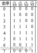
14N Twisted ring counter composed of bit trigger , How many independent states are there ?
Toroidal counter , Also known as Johnson counter , Only one trigger will flip every time the state changes , There is no competition or risk , stay n(n≥3) In the bit counter , You can use 2n Status , Yes 2n-2n Status not used
Verilog Code : Move right ,[0] Take the reverse and fill the high position
module johnson_cnt(
	input clk,
	input rst_n,
	output reg [3:0] out
	);

	always @(posedge clk or negedge rst_n) begin
		if(!rst_n) begin
			out <= 4'b0;
		end
		else begin
			out <= {
    ~out[0], out[3:1]} ;
		end
	end

endmodule
15 What structured description ? Description of behavior ? Data flow description ?
Data flow description : use assign Quotation of continuous assignment .
Description of behavior : Use always Sentence or initial Quotation of procedure assignment in statement block
Structured description : Instantiate existing function modules or primitives
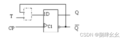
16 In order to achieve D Trigger conversion to T trigger , What circuit should be in the dotted box in the figure ?
17 There is one FIFO Design , Input clock 100Mhz, Output clock 80Mhz, The input data pattern is fixed , among 1000 There are... In each clock 800 A clock transmits continuous data , in addition 200 A free time , Excuse me, in order to avoid FIFO underflow / Overflow , What's the minimum depth
边栏推荐
- Differences between rip and OSPF and configuration commands
- 6.关于jwt
- 我感觉被骗了,微信内测 “大小号” 功能,同一手机号可注册两个微信
- Nat address translation
- App capture of charles+drony
- 伺服力矩控制模式下的力矩目标值(fTorque)计算
- How to choose the appropriate automated testing tools?
- DataSimba推出微信小程序,DataNuza接受全场景考验? | StartDT Hackathon
- 2022-07-04 matlab读取视频帧并保存
- ip netns 命令(备忘)
猜你喜欢

Improve application security through nonce field of play integrity API
![[paper sharing] where's crypto?](/img/27/9b47bfcdff8307e63f2699d6a4e1b4.png)
[paper sharing] where's crypto?

卖空、加印、保库存,东方甄选居然一个月在抖音卖了266万单书

Tips for short-term operation of spot silver that cannot be ignored

DataSimba推出微信小程序,DataNuza接受全场景考验? | StartDT Hackathon

企业展厅设计中常用的三种多媒体技术形式
小试牛刀之NunJucks模板引擎

Antisamy: a solution against XSS attack tutorial
Cadre de validation des données Apache bval réutilisé
![Learn open62541 -- [67] add custom enum and display name](/img/98/e5e25af90b3f98c2be11d7d21e5ea6.png)
Learn open62541 -- [67] add custom enum and display name
随机推荐
链式二叉树的基本操作(C语言实现)
将模型的记忆保存下来!Meta&UC Berkeley提出MeMViT,建模时间支持比现有模型长30倍,计算量仅增加4.5%...
Rules for filling in volunteers for college entrance examination
unity2d的Rigidbody2D的MovePosition函数移动时人物或屏幕抖动问题解决
RIP和OSPF的区别和配置命令
Reuse of data validation framework Apache bval
线程池中的线程工厂
清华、剑桥、UIC联合推出首个中文事实核查数据集:基于证据、涵盖医疗社会等多个领域
回归问题的评价指标和重要知识点总结
PTA 1101 B是A的多少倍
Reinforcement learning - learning notes 8 | Q-learning
[paper sharing] where's crypto?
Charles+Postern的APP抓包
[sword finger offer] 59 - I. maximum value of sliding window
SQLite SQL exception near "with": syntax error
Is it safe to open an online futures account now? How many regular futures companies are there in China?
Hash, bitmap and bloom filter for mass data De duplication
idea彻底卸载安装及配置笔记
Discuss | what preparations should be made before ar application is launched?
The performance and efficiency of the model that can do three segmentation tasks at the same time is better than maskformer! Meta & UIUC proposes a general segmentation model with better performance t