当前位置:网站首页>[esp32 learning-2] esp32 address mapping
[esp32 learning-2] esp32 address mapping
2022-07-06 12:03:00 【csdndulala】
This article begins with esp32 Technical reference manual A description in
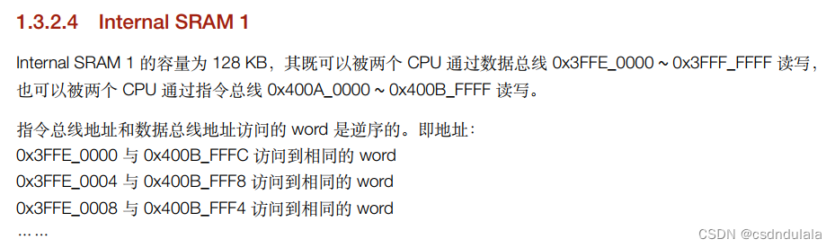
1.3.2.4 Internal SRAM 1
Internal SRAM 1 The capacity of is 128 KB, It can be divided into two CPU Via data bus 0x3FFE_0000 ~ 0x3FFF_FFFF Reading and writing ,
Can also be two CPU Via instruction bus 0x400A_0000 ~ 0x400B_FFFF Reading and writing .
Instruction bus address and data bus address access word It's in reverse order . The address :
0x3FFE_0000 And 0x400B_FFFC Access the same word
0x3FFE_0004 And 0x400B_FFF8 Access the same word
0x3FFE_0008 And 0x400B_FFF4 Access the same wordThe puzzle is why inter SRAM 1 Access different addresses through the data and instruction bus , Get the same content ? Why is this design ? What are the benefits ?
Search for information , Finally found Accurate answer : It can be customized IRAM and DRAM Size .( At the same time, it also solves ,esp32 Inside ram How to divide and use )ROM0 Why do I need Remap:
1.3.2.1 Internal ROM 0
Internal ROM 0 The capacity of is 384 KB, Can be two CPU Via instruction bus 0x4000_0000 ~ 0x4005_FFFF Read .
visit ROM 0 The head of the 32 KB The address of (0x4000_0000 ~ 0x4000_7FFF) Can be Remap To Internal SRAM 1 One of them
branch , This part was originally addressed 0x400B_0000 ~ 0x400B_7FFF visit . When remapping , this 32 KB SRAM Can no longer be addressed
0x400B_0000 ~ 0x400B_7FFF visit , however It can be used by data bus (0x3FFE_8000 ~ 0x3FFE_FFFF) visit . The way to do it is
There are two CPU Configure a register , That is to say PRO_CPU Set up DPORT_PRO_BOOT_REMAP_CTRL_REG The register of
bit 0 Or for APP_CPU Set up DPORT_APP_BOOT_REMAP_CTRL_REG The register of bit 0.There is no explanation on the Internet , I understand it :
rom0 As an instruction space, there are 384KB( It's already very big ), The allocated address space will not be fully used , Can pass remap The way , take rom The address of is mapped to ram The address of . This will speed up First level bootstrap Operation of .
Strongly recommended relevant information :
1 Memory address mapping
2 Flash state 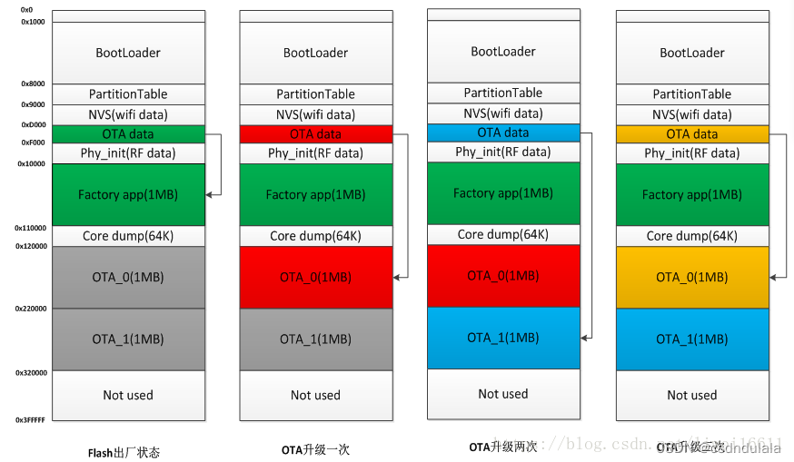
边栏推荐
- XML file explanation: what is XML, XML configuration file, XML data file, XML file parsing tutorial
- Unit test - unittest framework
- Variable star user module
- C语言,log打印文件名、函数名、行号、日期时间
- Gallery之图片浏览、组件学习
- Redis面试题
- Several declarations about pointers [C language]
- Mysql database interview questions
- [NPUCTF2020]ReadlezPHP
- Comparison of solutions of Qualcomm & MTK & Kirin mobile platform USB3.0
猜你喜欢

Mysql的索引实现之B树和B+树

A possible cause and solution of "stuck" main thread of RT thread
FTP文件上传文件实现,定时扫描文件夹上传指定格式文件文件到服务器,C语言实现FTP文件上传详解及代码案例实现
Priority inversion and deadlock

open-mmlab labelImg mmdetection
程序员老鸟都会搞错的问题 C语言基础 指针和数组
ToggleButton实现一个开关灯的效果
Unit test - unittest framework
Oppo vooc fast charging circuit and protocol

PyTorch四种常用优化器测试
随机推荐
Composition des mots (sous - total)
Gallery's image browsing and component learning
ARM PC=PC+8 最便于理解的阐述
使用LinkedHashMap实现一个LRU算法的缓存
STM32 how to locate the code segment that causes hard fault
I2C总线时序详解
Detailed explanation of express framework
MySQL START SLAVE Syntax
TypeScript
AMBA、AHB、APB、AXI的理解
机器学习--决策树(sklearn)
冒泡排序【C语言】
arduino获取随机数
Internet protocol details
分布式事务的实现方案
Cannot change version of project facet Dynamic Web Module to 2.3.
XML文件详解:XML是什么、XML配置文件、XML数据文件、XML文件解析教程
Reading notes of difficult career creation
MP3mini播放模块arduino<DFRobotDFPlayerMini.h>函数详解
优先级反转与死锁