当前位置:网站首页>Several important parameters of LDO circuit design and type selection
Several important parameters of LDO circuit design and type selection
2022-07-05 08:07:00 【Learning notes of hardware Xiaobai】
In the process of hardware device development , I believe many engineers will use LDO. mention LDO, The corresponding is DC-DC. The two are often compared . Xiaobai had an interview last summer , There are many questions about the differences between the two and their respective advantages and disadvantages .LDO Relatively speaking, it is still very common , Today, Xiaobai will talk about LDO.
LDO(Low-Dropout Linear Regulator) Low dropout linear regulator . As one of the most important circuit modules in hardware design , Many people must have used . Whether it's an integrated chip or a module built by yourself , Everyone should know something .
First of all, let's talk about , Using error amplifier to build a separate LDO.
The picture shows the simplest LDO Circuit diagram .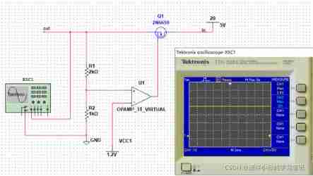
Mainly applied to , Error amplifier ,NMOS tube , resistance .
about OUT Calculation of terminal voltage , According to the virtual short and virtual break of operational amplifier , Calculate its OUT The value is 3.6V, It is mainly related to the reference voltage VCC1 as well as R1,R2 of . So this LDO The circuit diagram is mainly used for 5V turn 3.6V.
This circuit mainly uses MOS The variable resistance of the tube keeps the output voltage stable . When the later stage load is caused by other unstable factors OUT When the terminal voltage rises , here , Its partial voltage is given to the... Of the error amplifier “+” The voltage of stage becomes larger , As a result, the voltage difference with the negative reference voltage becomes larger , According to the operational amplifier Uo=A*(U±U-) It can be seen that the output voltage increases .MOS The tube works in the variable resistance area , At this time, the resistance increases , Make the circuit voltage difference larger , the OUT The terminal voltage drops down to keep the output stable .
I said before. , The output voltage is mainly related to the reference voltage and R1 R2 relevant . But the input voltage can not be arbitrary . According to the output voltage 3.6V namely MOS Tubular S Pole voltage is 3.6V, as well as MOS Tubular Uds The breakdown voltage of , We can calculate the maximum input voltage .
Chip aspect , Relatively integrated . manufacture LDO There are many chip manufacturers, such as TI,UTC, Ai Wei ,ETA etc. . Among them, Xiaobai used LDO Manufacturers have AI Weihe ETA.
Different manufacturers , Different models LDO, Its internal structure is different , There are often differences in circuit design . But the principle is the same as the above separation . It's just integrated into the chip .
Although the internal structure is different , But after all, when studying , The main parameters concerned are those , Now let's talk about LDO Several key parameters of .( Take AI as AW37030D180DNR Model number LDO As the case described this time )
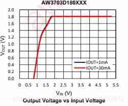
- Input & Output voltage
When selecting the model , The first concern is LDO The input of & Output voltage . Often refer to the manual LDO The input value of is often a range , The output is a fixed value .
Its input range is 1.9V-5V. But its output is 1.8V.
- Power rejection ratio
Express LDO The ability to suppress noise at the input . On many occasions ,LDO It's connected DC-DC Behind the circuit , Its main purpose is to suppress noise .
PSRR=20lg[(Vin-Vripple)/( Vout-Vripple)]
high PSRR Of LDO The inhibitory effect on the output ripple is still obvious .
We often datesheet See a curve like this on .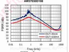
100K To 1MHz Internal PSRR It's very important , This is DCDC Noise frequency range ,LDO Often as DCDC Next level , Have the ability to filter out from DCDC A lot of noise .
stay ADC,DAC,Camera Of AVDD Power supply , We have to choose PSRR Greater than 80dB(@100Hz) Of LDO
- Rated output current
That is, through LDO Rated current . In design , Especially to this point . At the same time LDO Of datesheet On , We often see the current voltage curve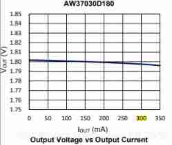
We can see from the picture The same LDO, Under different currents , Its output voltage value will also change slightly .
- LDO Temperature performance
Many electronic components have a specified working temperature range ,LDO It's also . Different packages have different temperature performance .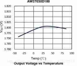
As you can see from the diagram , It is similar to the current value , In different circumstances , Yes LDO The output of has different effects .
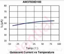
Quiescent current I Q
That is, the external load current is 0 when ,LDO The current required to supply power to the internal circuit . among , Quiescent current will be affected by external input voltage and temperature . As shown in the figure .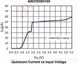
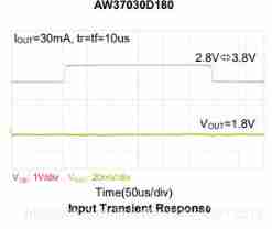
Transient response
stay LDO Application , Sometimes the input voltage and output load will change dramatically .LDO The input terminal of may be caused by the voltage fluctuation of the power supply equipment LDO The voltage at the input of... Changes dramatically . Output load switching may occur at the output end , Some load starts or stops . All of these will cause LDO The output voltage fluctuates . We can go through LDO The transient response curve of LDO When the input voltage or load current changes dramatically LDO Change of output voltage . With good transient response LDO, When the input voltage or load current changes dramatically ,LDO The fluctuation range of output voltage is small , Fast recovery time .
When the load current changes sharply , The output voltage is also very stable .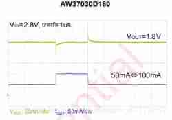
From the picture , We can see that when the input voltage changes sharply ,LDO The output of is hardly affected .
Circuit design 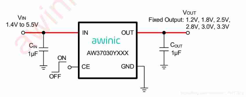
LDO It is divided into four pins , Respectively input and output , Enable and ground terminals .
IN Terminate the power input , for example DC-DC Output terminal or other power supply terminal , At the same time, the input terminal is connected with a small capacitor .
OUT Terminate the load . At the same time, connect a small capacitor .
CE Even if you can end ,LDO Work or not , You can observe whether the enable terminal is at high level .
GND Terminal grounding .
In circuit design , Hang a capacitor grounding at the input and output terminals , Better transient response can be obtained , At the same time, it also plays the role of filtering . For the choice of capacitance ,datesheet It is often referred to in , We can choose a given reference when designing .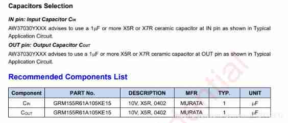
边栏推荐
- Network port usage
- Halcon's practice based on shape template matching [2]
- C language # and #
- IEEE access personal contribution experience record
- Reasons for rapid wear of conductive slip rings
- Consul installation
- Makefile application
- VESC Benjamin test motor parameters
- Wifi-802.11 negotiation rate table
- Hardware 1 -- relationship between gain and magnification
猜你喜欢
Network communication model -- Network OSI tcp/ip layering
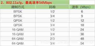
Wifi-802.11 negotiation rate table
Markdown tips
【论文阅读】2022年最新迁移学习综述笔注(Transferability in Deep Learning: A Survey)
C language enhancement -- pointer
![Correlation based template matching based on Halcon learning [II] find_ ncc_ model_ defocused_ precision. hdev](/img/42/d857452ccfeccbbf1ac34f47e47e2e.jpg)
Correlation based template matching based on Halcon learning [II] find_ ncc_ model_ defocused_ precision. hdev
List of linked lists
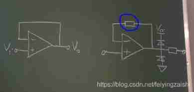
Hardware 3 -- function of voltage follower
C, Numerical Recipes in C, solution of linear algebraic equations, LU decomposition source program
![[trio basic tutorial 18 from introduction to proficiency] trio motion controller UDP fast exchange data communication](/img/05/0f63e4cd3da24e5b956ec5899b939d.jpg)
[trio basic tutorial 18 from introduction to proficiency] trio motion controller UDP fast exchange data communication
随机推荐
Random function usage notes
Some errors in configuring the environment
Shape template matching based on Halcon learning [v] find_ cocoa_ packages_ max_ deformation. Hdev routine
Halcon's practice based on shape template matching [1]
Altium designer 19.1.18 - Import frame
1-stm32 operation environment construction
Baiwen 7-day smart home learning experience of Internet of things
Improve lighting C program
Fundamentals of C language
DokuWiki deployment notes
How to copy formatted notepad++ text?
C language # and #
Record the visual shock of the Winter Olympics and the introduction of the screen 2
Altium designer 19.1.18 - clear information generated by measuring distance
Semiconductor devices (I) PN junction
Measurement fitting based on Halcon learning [III] PM_ measure_ board. Hdev routine
Win10 shortcut key
My-basic application 1: introduction to my-basic parser
Drive LED -- GPIO control
Shell脚本基本语法