当前位置:网站首页>PCB wiring rules of PCI Express interface
PCB wiring rules of PCI Express interface
2022-07-07 23:24:00 【ltqshs】
1. Impedance requirements
PCI-Express The routing impedance of the interface is 4 Layer or 6 The laminate must be kept 100 Difference (±20% MAX)/60 Single ended (±15%).
2. Line width and line spacing
Through impedance calculation software , combination PCB Stacking condition , Calculate the reasonable line width and line distance . such as , In the case of microstrip , The width of the difference line is 5mil, Differential alignment 2 The distance between the lines is 7mil.( In the case of striplines , The width of the difference line is 5mil, Differential alignment 2 The distance between the lines is 5mil.)
The distance between the difference pairs and the difference line with other non PCI Express Keep the distance of the signal 20mil Or four times the thickness of the medium , Choose the larger one . If the PCI Express The signal voltage is significantly higher than or not PCI EXPRESS Signal edge ratio PCI Express If the signal edge is fast , The space for both should be increased to 30mil, To avoid coupling . Pictured 1 Shown :
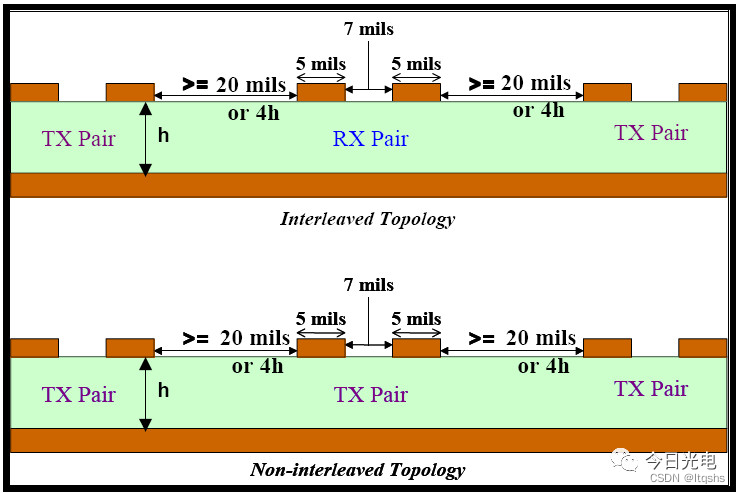
chart 1
3. Length and length match
In order to disperse the influence of the effective thickness area of the glass fiber bundle braid and the non reinforced surface resin layer of the dielectric layer , Long distance routing must be consistent with XY The axis is at an oblique angle ( The long line should be slashed on the board ), Pictured 2 Shown :
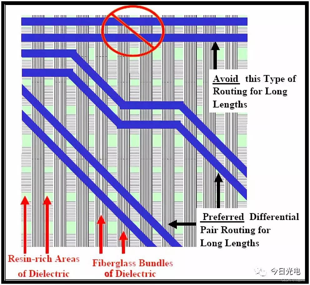
chart 2
PCB Per inch routing may be introduced 1ps5ps Jitter budget and 0.25dB0.35dB Loss of . The medium is FR4 Of PCB, Generally speaking :
a. The maximum routing of the differential pair from chip to chip cannot exceed 6 Inch ;
b. The difference between the lengths of the two routes in the differential pair should be less than or equal to 5mil.
When encountering special situations such as tight layout, the routing can be done by 5-7 Become smaller line width and line spacing , But when that happens , The routing length of the transformed differential pair cannot exceed 150mil. Pictured 3 Shown :
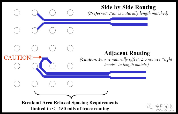
chart 3
Also, the length matching should be as close to the signal pin as possible without introducing any small angle bending . Refer to figure for specific routing 4:
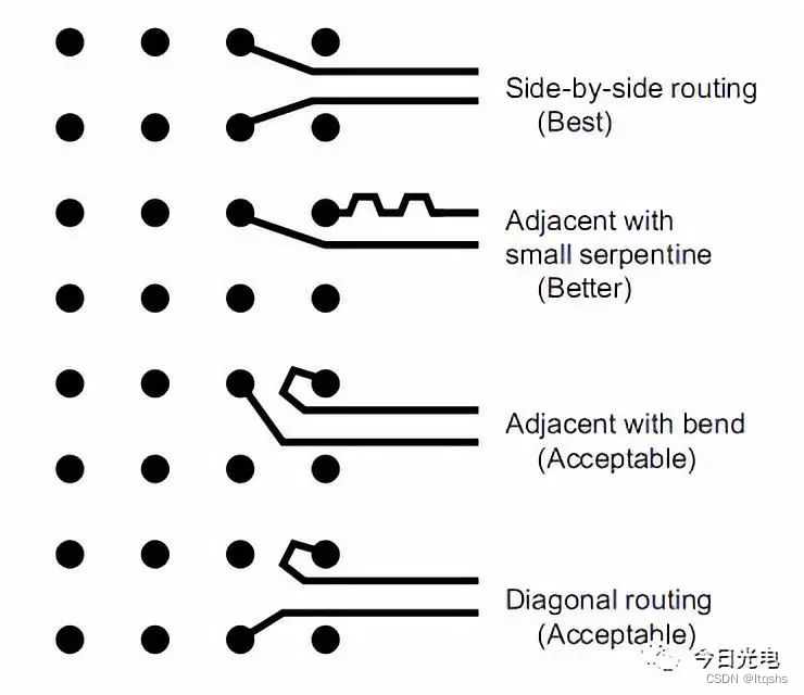
chart 4
4. Test point 、 Vias and pads
Signal vias affect the overall loss and jitter budget , Limit the maximum routing length .
stay TX Differential alignment can be used at most 4 Two vias , And in the RX Differential alignment can only be used at most 2 Two vias . There should be a through hole 25mil Or smaller pads , And its finished inner diameter should be 14mil Or less . The two vias must be placed in a symmetrical position . Pictured 5 Shown :
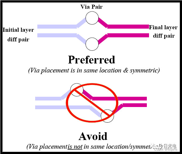
chart 5
Test point ( It can be via , Pads or components ) And the probe foot should be placed in a symmetrical position , Should not be introduced in differential pairs stub, Pictured 6:
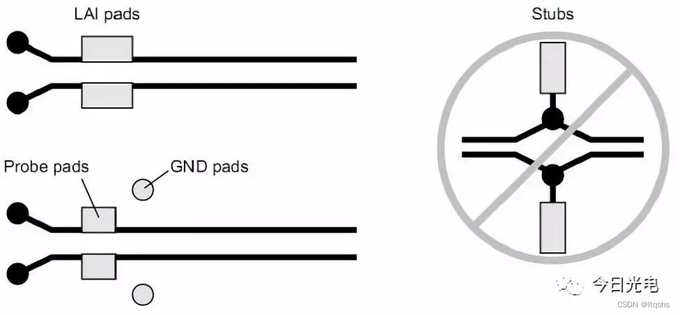
chart 6
5. bending
Try not to use bending , Because it will introduce common mode noise . The following rules should be followed when using bending for differential pairs :( In an effort to 7 For example )
1. All bending angles (α) should ≥135°;
2. Maintain line spacing (A)≥20mil;
3. fragment , such as B and C, Its flank has a bend , Its length should be ≥1.5 Times the wiring width .
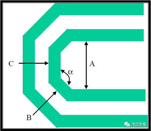
chart 7
Try to make the number of left bends equal to the number of right bends .
When a serpentine line is used to match the length of another line , The length of each long bend must be at least 15mil(3 Twice as much as 5mil The line width of ). The maximum distance between the bending part of the serpentine and the other line of the differential line must be less than that of the normal differential line 2 times . Pictured 8 Shown :
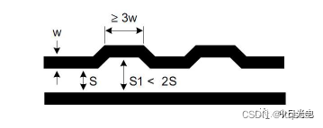
chart 8
When using multiple bend wiring to a pin or a BGA The unmatched part of the pad of should ≤45mil, Pictured 9 Shown :
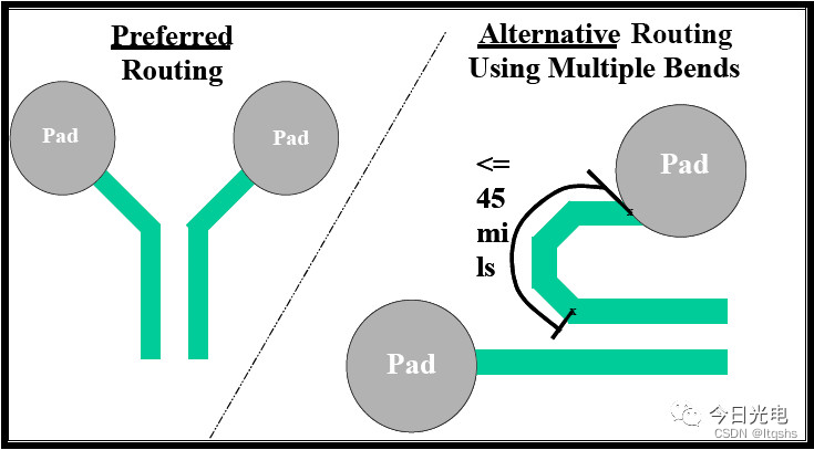
chart 9
The bending curve connected to the pad should follow the following rules :( In an effort to 10 For example )
1. All bending angles (α) should ≥135°;
2. Maintain line spacing (A)≥3 Times the wiring width ;
3.B and C The length of the segment should be ≥1.5 Times the wiring width ;
4.D The paragraph should be as short as possible .
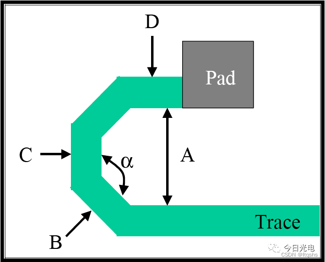
chart 10
6.AC capacitance
PCIExpress AC coupling between the sending end and the receiving end is required . The difference must have the same capacitance value for the AC coupling capacitance of the two signals , Same package size , And the position is symmetrical .
AC The capacitor must be placed closest to the signal sending end . Capacitance value must be between 75nF To 200nF Between ( It is best to 100nF). Recommended 0402 encapsulation , however 0603 Encapsulation is also acceptable . The two capacitors should be placed symmetrically , Pictured 11 Shown :
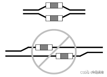
chart 11
In addition, the differential reference clock should use the same differential line with the same geometric structure as the high-speed serial data line .
See the original text :《PCI-Express Wiring rules of the interface 》
边栏推荐
- 网络安全-永恒之蓝
- Adrnoid开发系列(二十五):使用AlertDialog创建各种类型的对话框
- The 19th Zhejiang Provincial College Programming Contest 2022 f.easyfix chairman tree
- PCI-Express接口的PCB布线规则
- leetcode-520. 检测大写字母-js
- 云原生正在吞噬一切,开发者该如何应对?
- 伸展树(一) - 图文解析与C语言实现
- 648. 单词替换
- Matlab SEIR infectious disease model prediction
- 给出一个数组,如 [7864, 284, 347, 7732, 8498],现在需要将数组中的数字拼接起来,返回「最大的可能拼出的数字」
猜你喜欢
![MATLAB signal processing [Q & A essays · 2]](/img/be/0baa92767c3abbda9b0bff47cb3a75.png)
![给出一个数组,如 [7864, 284, 347, 7732, 8498],现在需要将数组中的数字拼接起来,返回「最大的可能拼出的数字」](/img/21/2e99dd6173ab4925ec22290cd4a357.png)
随机推荐
The 19th Zhejiang Provincial College Programming Contest VP record + supplementary questions
USB(十四)2022-04-12
Inftnews | web5 vs Web3: the future is a process, not a destination
Cloud native is devouring everything. How should developers deal with it?
成年人只有一份主业是要付出代价的,被人事劝退后,我哭了一整晚
Unity3d learning notes 5 - create sub mesh
Network security - joint query injection
Network security - phishing
Why does the market need low code?
Wechat forum exchange applet system graduation design completion (1) development outline
LDO穩壓芯片-內部框圖及選型參數
PCI-Express接口的PCB布线规则
sql 数据库执行问题
Dynamics 365 find field filtering
13、 System optimization
Quelles sont les similitudes et les différences entre les communautés intelligentes et les villes intelligentes?
漏洞复现----49、Apache Airflow 身份验证绕过 (CVE-2020-17526)
Introduction to redis and jedis and redis things
Install a new version of idea. Double click it to open it
Gee (III): calculate the correlation coefficient between two bands and the corresponding p value