当前位置:网站首页>Jesd204b clock network
Jesd204b clock network
2022-07-07 07:08:00 【MDYFPGA】
This article is an original article by Ming Deyang , Reprint please indicate the source !
Mingdeyang's JESD204B After the acquisition card project is integrated on the board , You can use the upper computer to configure through Gigabit Network AD9144 and AD9516 card , High speed ad collection . Finally, the sine wave of the set frequency can be collected on the oscilloscope and the upper computer . This article focuses on JESD204B Clock network .
One ,JESD204B Overview of clock network principle
This article takes JESD204B subclass1 To discuss the timing needs of the clock and TI Implementation of clock chip scheme . Any serial protocol cannot be separated from frame and synchronization ,JESD204B No exception , It also requires the same frame structure between the sender and the receiver , Then synchronize in a way , That is, identify the beginning .JESD204B It uses the edge of the clock signal to identify the beginning of synchronization , And through a certain handshake signal, both the sender and the receiver can correctly identify the length and boundary of the frame , Therefore, the clock signal and its timing relationship are important for JESD204B It is extremely important . The figure below is typical of JESD204B System connection of the system :

Device Clock It is the master clock of the device , Generally, it is a sampling clock or an integer frequency doubling clock in a digital to analog converter , The frame of the protocol itself and the clock of multiple frames are also based on Device Clock.SYSREF It is used to indicate different converters or logic Device Clock Edge of , Or between different devices Deterministic latency The reference of . As shown in the figure below ,Device Clock and SYSREF The temporal relationship that must be satisfied .

SYSREF The first rising edge of must be very easy to be Device Clock Catch , This requires SYSREF and Device Clock Meet the timing relationship in the above figure . Usually because of PCB The length of the line and the output of different channels of the clock device Skew, It will bring some errors ,Device Clock The rising edge of does not necessarily coincide with SYSREF In the middle of the pulse , As long as the project is within a certain range, it can be guaranteed JESD204 The transceiver works normally .
Two , Ming Deyang JESD204B Project clock network introduction
Ming Deyang JESD204B Acquisition card project use Xilinx Of KC705 Development board , disjunctive DA The board contains ad9144 Chips and ad9516 Clock chip .
The project consists of FPGA Send a source clock to ad9516 chip , Then by ad9516 Chip output 4 A clock , among 2 A clock is sent to FPGA, in addition 2 A clock is sent to ad9144 chip . The specific structure is as follows :

AD9516 Introduce
AD9516, This is a result of ADI Designed by the company 14 Output clock generator , It has sub picosecond jitter performance , It is also equipped with on-chip integrated phase-locked loop (PLL) And voltage controlled oscillator (VCO). Intraslice VCO The tuning frequency range is 2.55 GHz to 2.95 GHz. perhaps , The highest... Can also be used 2.4 GHz The outside of the VCO/VCXO.
AD9516 Yes 6 road (3 Yes )LVPECL Output ,4 road (2 Yes )LVDS Output and 8 road LVCMOS( Every LVDS It can be used as 2 road LVCMOS) Output . The shared value between each pair is 1-32 Frequency division value of , therefore , Each pair LVPECL perhaps LVDS The output clock frequency is the same .LVPECL The output can reach 1.6GHz,LVDS The output can reach 800MHz,LVCMOS Can be up to 250MHz. Enter the reference clock frequency and VCO The working frequency has something to do with : Fvco=(Fref/R)*(P*B+A)
Each output has a single frequency division factor (1-32) You can configure the , Through the selection of reference clock , Inside P、B、A Register and the configuration of each frequency division register , We can get the clock we want .
The above is about mingdeyang JESD204B Introduction of clock network , Mingdeyang can undertake based on JESD204B High speed data transmission project , To learn more , Interested students can leave messages to discuss with each other !
边栏推荐
- 2022/07/04学习记录
- Four goals for the construction of intelligent safety risk management and control platform for hazardous chemical enterprises in Chemical Industry Park
- JWT的基础介绍
- 服装门店如何盈利?
- 2018 Jiangsu Vocational College skills competition vocational group "information security management and evaluation" competition assignment
- 请教一个问题,flink oracle cdc,读取一个没有更新操作的表,隔十几秒就重复读取全量数据
- RuntimeError: CUDA error: CUBLAS_ STATUS_ ALLOC_ Failed when calling `cublascreate (handle) `problem solving
- 【NOI模拟赛】区域划分(结论,构造)
- How can brand e-commerce grow against the trend? See the future here!
- 大咖云集|NextArch基金会云开发Meetup来啦
猜你喜欢
unity3d学习笔记
Config分布式配置中心
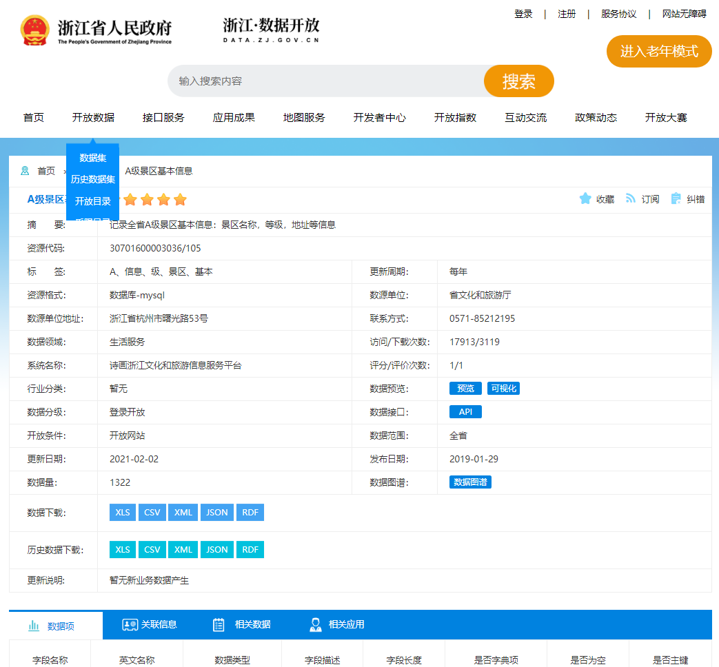
Data of all class a scenic spots in China in 2022 (13604)
关于数据库数据转移的问题,求各位解答下
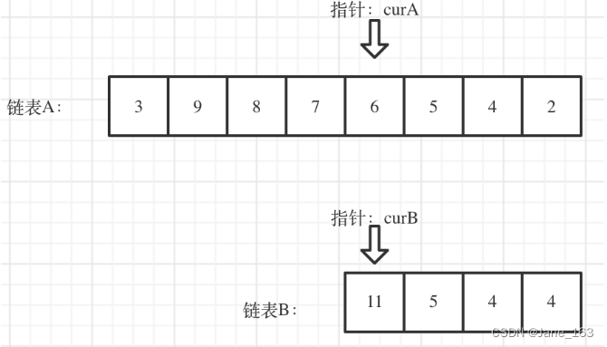
LC interview question 02.07 Linked list intersection & lc142 Circular linked list II
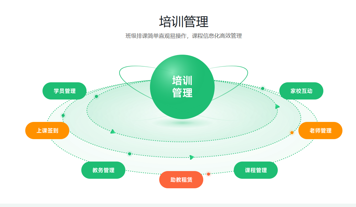
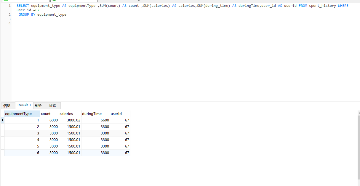
How to do sports training in venues?
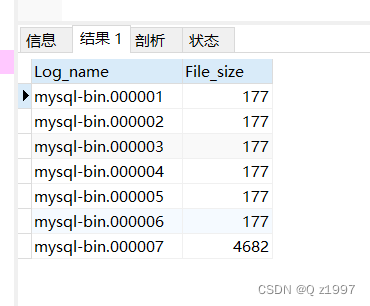
MySQL view bin log and recover data

大促过后,销量与流量兼具,是否真的高枕无忧?
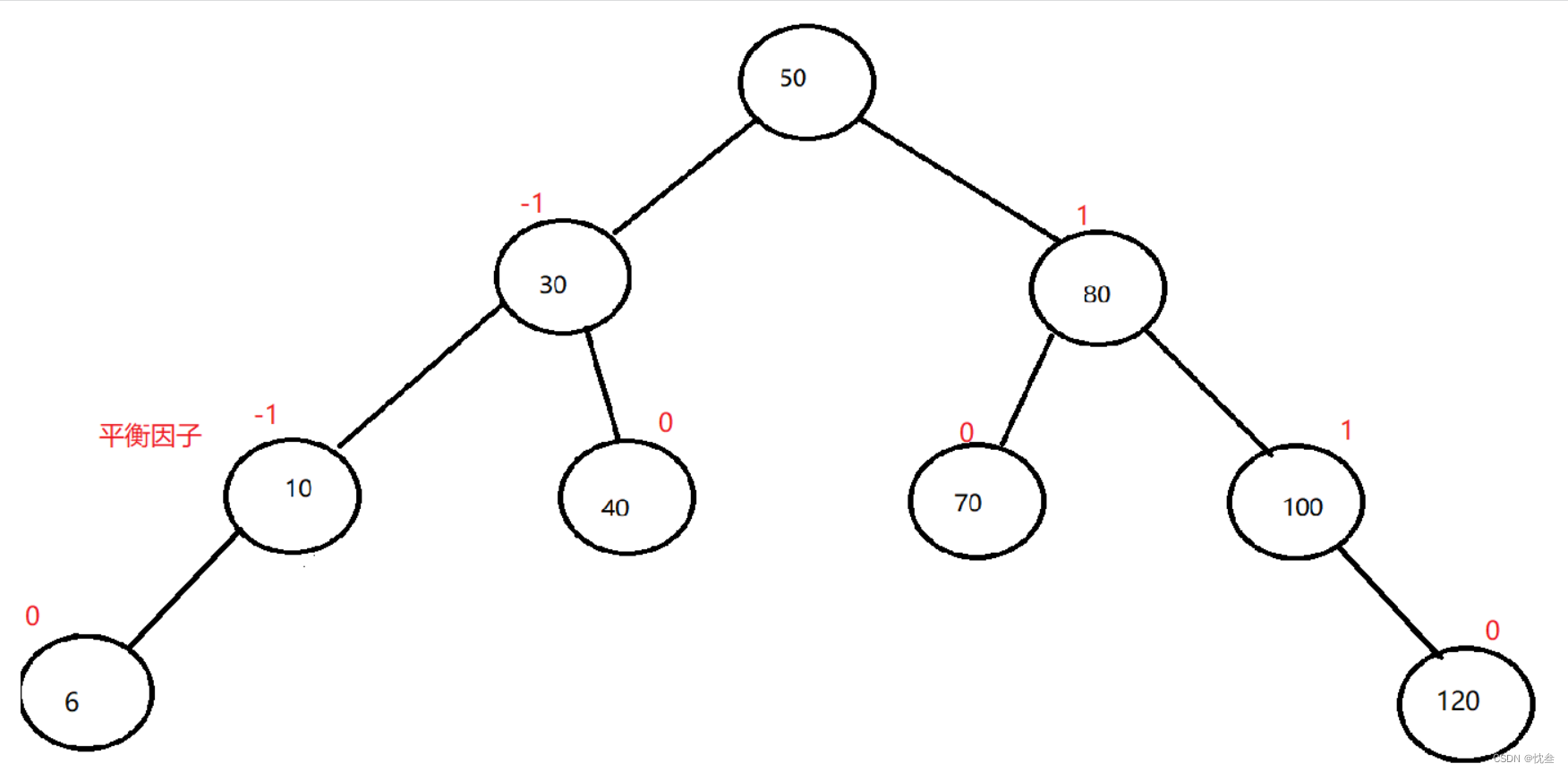
AVL树的实现
数据资产管理与数据安全国内外最新趋势
随机推荐
MySql用户权限
main函数在import语句中的特殊行为
LC interview question 02.07 Linked list intersection & lc142 Circular linked list II
Complete process of MySQL SQL
Comment les entreprises gèrent - elles les données? Partager les leçons tirées des quatre aspects de la gouvernance des données
使用net core优势/为什么使用
组件的嵌套和拆分
Matlab tips (29) polynomial fitting plotfit
Unity3d learning notes
华为机试题素数伴侣
mysql查看bin log 并恢复数据
Distributed ID solution
Basic process of network transmission using tcp/ip four layer model
toRefs API 与 toRef Api
SVN version management in use replacement release and connection reset
Please ask a question, flick Oracle CDC, read a table without update operation, and repeatedly read the full amount of data every ten seconds
根据IP获取地市
How can brand e-commerce grow against the trend? See the future here!
DHCP路由器工作原理
组件的通信