当前位置:网站首页>EDP to LVDS conversion design circuit | EDP to LVDS adapter board circuit | capstone/cs5211 chip circuit schematic reference
EDP to LVDS conversion design circuit | EDP to LVDS adapter board circuit | capstone/cs5211 chip circuit schematic reference
2022-07-08 01:09:00 【qq1659747718】
CS5211–DP to LVDS
DisplayPort To LVDS converter
Two channels DP Input , Double link LVDS Output
CS5211 Is a display port To LVDS Converter design PC machine , utilize GPU And display port (DP) Or embedded display port (eDP) Output and acceptance LVDS Display panel for input .
CS5211 The main features
Use of tape is allowed DisplayPort Of LVDS Display panel or eDP Video source device
Support 1920×[email protected] when 24 Metachromatic depth
Parade Of CrystalFree No external crystal or time reference is required technology
A single 3.3V or 2.5V Low power supply ,1920×400mW following [email protected] when , Each pixel 24 position
The dual power option is I/O Use 3.3V or 2.5V, Core use 1.35V or 1.2V
No firmware operation , Support hardware pin configuration or initial code configuration
Optional I2C host , For external use EEPROM Initial code loading and device configuration
Chip controlled optional I2C From the interface
ESD:HBM 8kV at Connector pins
Operating temperature range availability :-20°C to 70°C( commercial ),-40° to 85°C( Industry )
7x7mm 56 The needle QFN encapsulation ( Halogen-free , accord with RoHS)
DisplayPort Input
accord with VESA DisplayPort standard 1.1a
Support 18、24 and 30 bpp RGB Color format input
Including tape integration HDCP secret key ROM Of HDCP 1.3 Decryption engine
accord with VESA Embedded display port (eDP) standard 1.2, With auxiliary start backlight control
Support 1 Channels and 2 Channel master connection configuration
1.62 Gbps and 2.7Gbps Link rate
Supports a variety of... Specific GPU Power management protocol
Support all eDP Show Authentication Scheme , Include ASSR
Support SSC 0.5% Downward expansion
Support full link training 、 Quick link training and unlinked training
Low voltage differential signal interface
Single link or double link LVDS Output , Clock speeds up to 135MHz
Support 1920×[email protected] when 18 or 24 Metachromatic depth
LVDS Spread spectrum clock frequency up to 2%
Support LCD Panel power sequence control
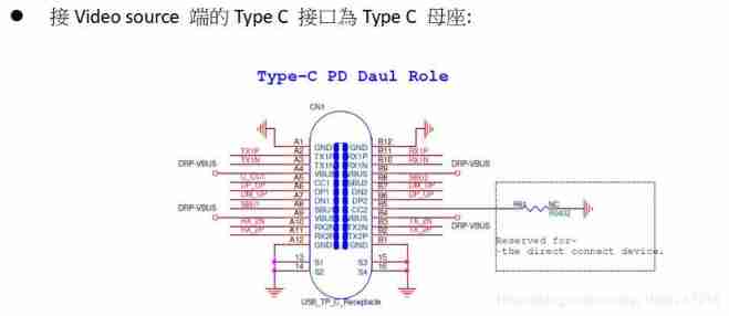
CS5211 Design EDP to LVDS Convert the reference circuit or EDP to LVDS The adapter board reference circuit is shown below :


CS5211 Design EDP to LVDS Converter or EDP to LVDS The design characteristics of the adapter plate are as follows :
CS5211 Will serve as a DP or eDP The receiver device appears in the video source , And will serve as LVDS Display panel LVDS Source device . The device is a fully integrated solution , No external is required CPU、 Memory 、 Clock reference or voltage regulator .CS5211 Can be configured to slave from the display DDC Channel or connect from to CS5211( Provide I2C host ) External options ROM Read EDID. external ROM It can also include configuration code , To customize equipment operation and interface timing .CS5211 Provide power on sequence of display panel and backlight control , Include PWM Generate . Backlight characteristics can be obtained by using eDP v1.2 DPCD Control register DP AUX Control the video source on the channel . perhaps , The video source can provide a backlight control signal to CS5211,CS5211 Gate it for panel power up sequencing , Alternatively, the video source can bypass the device and directly control the backlight of the panel .
边栏推荐
- [Yugong series] go teaching course 006 in July 2022 - automatic derivation of types and input and output
- 13. Enregistrement et chargement des modèles
- Vs code configuration latex environment nanny level configuration tutorial (dual system)
- 基础篇——整合第三方技术
- What does interface testing test?
- 10.CNN应用于手写数字识别
- Ag9310 for type-C docking station scheme circuit design method | ag9310 for type-C audio and video converter scheme circuit design reference
- For the first time in China, three Tsinghua Yaoban undergraduates won the stoc best student thesis award
- German prime minister says Ukraine will not receive "NATO style" security guarantee
- NTT template for Tourism
猜你喜欢
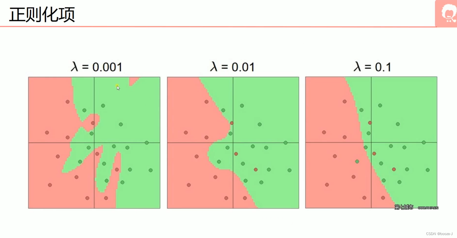
5.过拟合,dropout,正则化
My best game based on wechat applet development
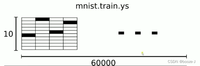
3. MNIST dataset classification
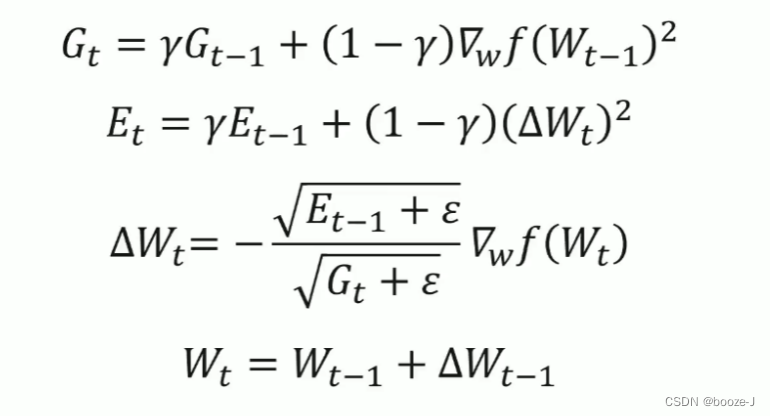
8.优化器

From starfish OS' continued deflationary consumption of SFO, the value of SFO in the long run
![[note] common combined filter circuit](/img/2f/a8c2ef0d76dd7a45b50a64a928a9c8.png)
[note] common combined filter circuit

Two methods for full screen adaptation of background pictures, background size: cover; Or (background size: 100% 100%;)

Markdown learning (entry level)
Vs code configuration latex environment nanny level configuration tutorial (dual system)
Ag9310 for type-C docking station scheme circuit design method | ag9310 for type-C audio and video converter scheme circuit design reference
随机推荐
[Yugong series] go teaching course 006 in July 2022 - automatic derivation of types and input and output
NTT template for Tourism
基于人脸识别实现课堂抬头率检测
C# ?,?.,?? .....
Swift get URL parameters
Semantic segmentation model base segmentation_ models_ Detailed introduction to pytorch
Complete model verification (test, demo) routine
Chapter XI feature selection
基于卷积神经网络的恶意软件检测方法
New library online | cnopendata China Star Hotel data
y59.第三章 Kubernetes从入门到精通 -- 持续集成与部署(三二)
利用GPU训练网络模型
14. Draw network model structure
Definition and classification of energy
9.卷积神经网络介绍
Several frequently used OCR document scanning tools | no watermark | avoid IQ tax
Class head up rate detection based on face recognition
133. 克隆图
手写一个模拟的ReentrantLock
[necessary for R & D personnel] how to make your own dataset and display it.