当前位置:网站首页>SPI details
SPI details
2022-07-05 06:06:00 【Bitongo】
List of articles
- One 、SPI brief introduction
- Two 、SPI Function description
- 3、 ... and 、SPI Register description
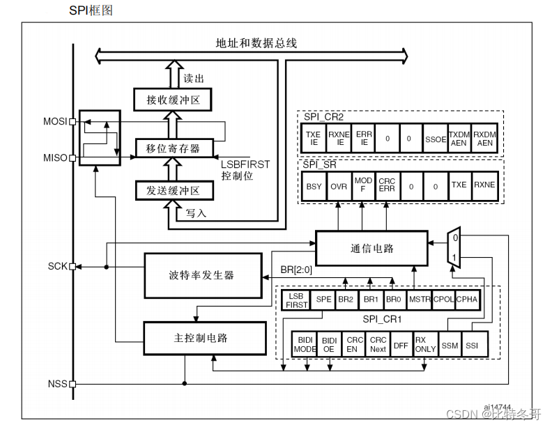
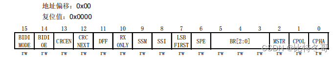
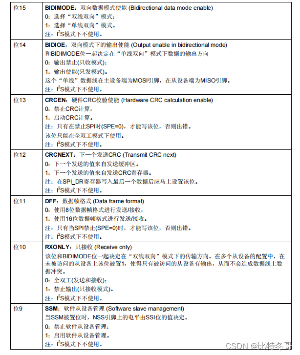
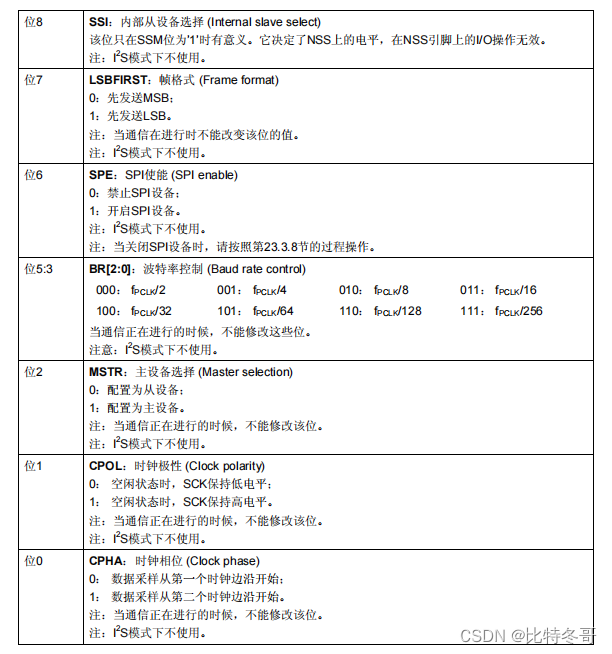
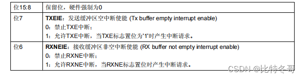
- 1. SPI Control register 1(SPI_CR1)
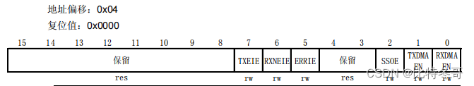
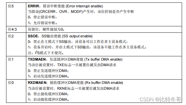
- 2. SPI Control register 2(SPI_CR2)
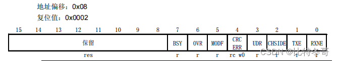
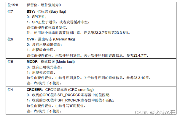
- 3. SPI Status register (SPI_SR)
- 4. SPI Data register (SPI_DR)
- 5. SPI CRC Polynomial register (SPI_CRCPR)
- 6. SPI Rx CRC register (SPI_RXCRCR)
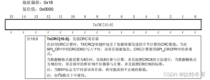
- 7. SPI Tx CRC register (SPI_TXCRCR)
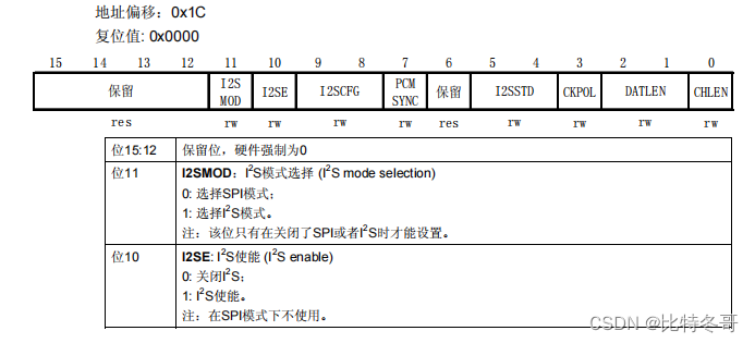
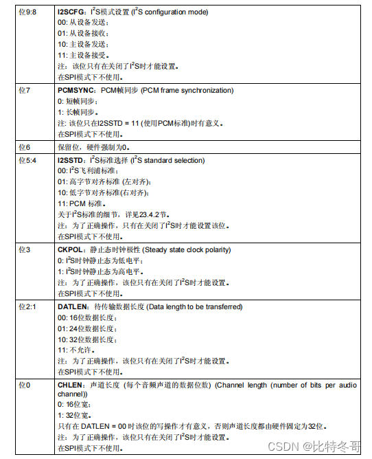
- 8. SPI_I2S Configuration register (SPI_I2S_CFGR)
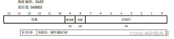
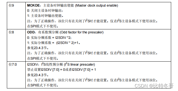
- 9. SPI_I2S Prescaler register (SPI_I2SPR)
- 10. SPI Register address mapping
One 、SPI brief introduction
SPI It's English Serial Peripheral interface Abbreviation , As the name implies, it is serial peripheral interface . yes Motorola First of all MC68HCXX Defined on the family processor .SPI The interface is mainly used in EEPROM,FLASH, Real time clock ,AD converter , And between the DSP and the DSP .SPI, It's a high speed , full duplex , Synchronous communication bus , And only four wires are used on the chip pins , Saved the chip pins , Also for PCB Save space on layout of , Convenient , It is out of this simple and easy-to-use feature , Now more and more chips integrate this communication protocol ,STM32 Also have SPI Interface .
features
● 3 Line full duplex synchronous transmission
● Two wire simplex synchronous transmission with or without the third bidirectional data line
● 8 or 16 Bit transmission frame format selection
● Master or slave operation
● Support multi master mode
● 8 Baud rate prescaler coefficient of main modes ( The maximum is fPCLK/2)
● From mode frequency ( The maximum is fPCLK/2)
● Fast communication between master mode and slave mode
● Both master mode and slave mode can be controlled by software or hardware NSS management : Lord / From the dynamic change of operation mode
● Programmable clock polarity and phase
● Programmable data sequence ,MSB In front or LSB before
● Dedicated send and receive flags that trigger interrupts
● SPI Bus busy status flag
● Hardware that supports reliable communication CRC
─ In send mode ,CRC The value can be sent as the last byte
─ In full duplex mode, the last byte received is automatically updated CRC check
● Main mode failure that triggers interrupts 、 Overload and CRC Error flag
● Support DMA Functional 1 Byte send and receive buffers : Generate send and receive requests
Two 、SPI Function description
1. summary
Usually SPI adopt 4 Pins are connected to external devices :
● MISO: Master input / Output pin from device . The pin sends data in slave mode , Receive data in main mode .
● MOSI: Main device output / Input from device pin . This pin sends data in main mode , Receive data in slave mode .
● SCK: Serial clock , Output as master device , Input from device
● NSS: Choose from the device . This is an optional pin , It's used to select the master / Slave device .
Its function is to serve as a “ Chip selection pin ”, Let the master device communicate with a specific slave device independently , Avoid conflicts on data lines . From the device's NSS The pin can be a standard by the master device I/O Pin to drive . Once enabled (SSOE position ),NSS Pin can also be used as output pin , And in SPI Pull down when in main mode ; here , be-all SPI equipment , If their NSS The pin is connected to the... Of the main device NSS Pin , Low level will be detected , If they are set to NSS Hardware mode , It will automatically enter the slave device state . When configured as the master device 、NSS Configured as input pin (MSTR=1SSOE=0) when , If NSS Pulled down , Then this SPI The device failed to enter the main mode : namely MSTR The bit is automatically cleared , This device enters slave mode ( See ) The following figure is an example of the interconnection of single master and single slave devices .
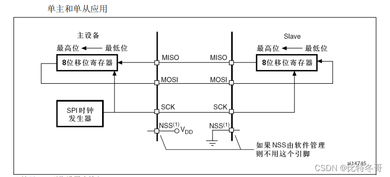
- here NSS Pin set to input
MOSI The feet are connected to each other ,MISO The feet are connected to each other . such , Data is transmitted serially between master and slave (MSB In front of ). Communication is always initiated by the master device . The main equipment passes through MOSI The foot sends data to the slave device , From the device through MISO Pin return data . This means that the data output and data input of full duplex communication are synchronized with the same clock signal ; The clock signal is passed by the master equipment SCK Feet provide .
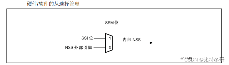
Select from (NSS) Foot management
Yes 2 Kind of NSS Pattern :
● Software NSS Pattern : Can be set by SPI_CR1 The register of SSM Bits enable this mode . In this mode NSS Pins can be used for other purposes , And inside NSS The signal level can be determined by writing SPI_CR1 Of SSI Bit to drive
● Hardware NSS Pattern , There are two situations :
─ NSS The output is enabled : When STM32F10xxx Work oriented SPI, also NSS The output has passed SPI_CR2 The register of SSOE Bit enable , At this time NSS The pin is pulled low , all NSS Pin with this master SPI Of NSS The pins are connected and configured as hardware NSS Of SPI equipment , Will automatically become from SPI equipment .
When one SPI The device needs to send broadcast data , It must be pulled down NSS The signal , To inform all other devices that it is the master device ; If it doesn't pull down NSS, This means that there is another master device communicating on the bus , A hardware failure error will be generated (Hard Fault).
─ NSS The output is turned off : Allow operation in multiple master environments .
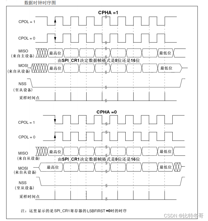
The phase and polarity of the clock signal
SPI_CR The register of CPOL and CPHA position , Can be combined into four possible temporal relationships .CPOL( Clock polarity ) Bit controls the idle state level of the clock when there is no data transmission , This bit is valid for both devices in master mode and slave mode . If CPOL By clear ’0’,SCK The pin remains low in the idle state ; If CPOL Be placed ’1’,SCK The pin remains high in the idle state .
If CPHA( Clock phase ) The bit is set ’1’,SCK The second edge of the clock (CPOL Position as 0 Time is the falling edge ,CPOL position by ’1’ Time is the rising edge ) Sampling data bits , The data is latched at the edge of the second clock . If CPHA Bit cleared ’0’,SCK The first edge of the clock (CPOL Position as ’0’ Time is the falling edge ,CPOL Position as ’1’ Time is the rising edge ) Perform data bit sampling , Data is latched at the edge of the first clock .
CPOL Clock polarity and CPHA The combination of clock phases selects the clock edge of data capture .
The following figure shows SPI Transmission of 4 Kind of CPHA and CPOL Bit combination . This figure can explain the... Of master device and slave device SCK foot 、MISO foot 、MOSI The master or slave sequence diagram with the feet directly connected .
Be careful :
- Changing CPOL/CPHA Bit before , Must be cleared SPE General SPI prohibit .
- Master and slave must be configured in the same timing mode .
- SCK The idle state of must be the same as SPI_CR1 The polarity specified by the register is consistent (CPOL by ’1’ when , Pull up when you are free SCK High level ;CPOL by ’0’ when , When idle, you should pull down SCK Low level ).
- Data frame format (8 Bit or 16 position ) from SPI_CR1 The register of DFF Bit selection , And decided to send / Length of data received .
Data frame format
according to SPI_CR1 In register LSBFIRST position , When outputting data bits, you can MSB You can also LSB First . according to SPI_CR1 The register of DFF position , Each data frame can be 8 Bit or 16 position . The selected data frame format is suitable for transmission and transmission / Or reception is valid .
2. To configure SPI For slave mode
In slave mode ,SCK The pin is used to receive the serial clock from the master device .SPI_CR1 In the register BR[2:0] The setting of does not affect the data transfer rate .
notes : It is recommended to enable before the master sends the clock SPI Slave device , Otherwise, unexpected data transmission may occur . Before the first edge of the communication clock arrives or the ongoing communication ends , The data register of the slave device must be ready . Before enabling the slave and master , The polarity of the communication clock must be at a stable value . Please follow the steps below to configure SPI For slave mode :
Configuration steps
- Set up DFF Bit to define the data frame format as 8 Bit or 16 position .
- choice CPOL and CPHA Bit to define the phase relationship between data transmission and serial clock . To ensure correct data transmission , Slave and master CPOL and CPHA Bits must be configured in the same way .
- The frame format (SPI_CR1 In register LSBFIRST A definition of ”MSB before ” still ”LSB before ”) It must be the same as the main equipment .
- In hardware mode ( Refer to select (NSS) Foot management ), In the complete data frame (8 Bit or 16 position ) During transmission ,NSS The pin must be low . stay NSS In software mode , Set up SPI_CR1 In register SSM Bit and clear SSI position .
- eliminate MSTR position 、 Set up SPE position (SPI_CR1 register ), Make the corresponding pin work in SPI In mode . In this configuration ,MOSI The pin is the data input ,MISO The pin is the data output .
Data transmission process
In write operation , Data words are written to the transmit buffer in parallel . When the clock signal is received from the device , And in MOSI When the first data bit appears on the pin , The sending process begins ( Translation notes : At this time, the first bit is sent ). The remaining bits ( about 8 Bit data frame format , also 7 position ; about 16 Bit data frame format , also 15 position ) Loaded into shift register . When the data in the transmit buffer is transferred to the shift register ,SPI_SP The register of TXE The logo is set , If set SPI_CR2 The register of TXEIE position , There will be an interrupt .
Data receiving process
For the receiver , When data reception is complete :
● The data in the shift register is transferred to the receive buffer ,SPI_SR In register RXNE The logo is set .
● If set SPI_CR2 In register RXNEIE position , Then there is an interruption .
After the edge of the last sampling clock ,RXNE The bit is set ’1’, The data bytes received in the shift register are transferred to the receive buffer . When reading SPI_DR When the register ,SPI The device returns the value of this receive buffer . read SPI_DR When the register ,RXNE Bit is cleared .
3. To configure SPI Main mode
In the main configuration , stay SCK The pin generates a serial clock .
Configuration steps
- adopt SPI_CR1 The register of BR[2:0] Bit defines serial clock baud rate .
- choice CPOL and CPHA position , Define the phase relationship between data transmission and serial clock .
- Set up DFF To define 8 Bit or 16 Bit data frame format .
- To configure SPI_CR1 The register of LSBFIRST Bit defines the frame format .
- if necessary NSS The pin works in input mode , In hardware mode , During the transmission of the whole data frame NSS Pin connected to high level ; In software mode , Need to set up SPI_CR1 The register of SSM Bit and SSI position . If NSS The pin operates in output mode , Then just set SSOE position .
- You have to set MSTR Bit and SPE position ( should only NSS The pin is connected to high level , These bits can remain set ). In this configuration ,MOSI The pin is the data output , and MISO The pin is the data input .
Data transmission process
When writing data to the transmit buffer , The sending process begins . When sending the first data bit , Data words are in parallel ( Through the internal bus ) Pass in shift register , And then move out serially to MOSI On the feet ;MSB First or LSB First , Depending on SPI_CR1 In register LSBFIRST Bit setting . When data is transferred from the transmit buffer to the shift register TXE The flag will be set , If set SPI_CR1 In register TXEIE position , There will be interruptions .
Data receiving process
For the receiver , When the data transmission is complete :
● Transfer the data in the shift register to the receive buffer , also RXNE The flag is set .
● If set SPI_CR2 In register RXNEIE position , Then there is an interruption .
At the last sampling clock edge ,RXNE Bit is set , The data word received in the shift register is transferred to the receive buffer .
read SPI_DR When the register ,SPI The device returns the data in the receive buffer .
read SPI_DR The register will be cleared RXNE position . Once the transmission starts , If the next data to be sent is put into the transmission buffer , A continuous transport stream can be maintained . Before attempting to write the transmit buffer , Need to confirm TXE The sign should be ’1’.
notes : stay NSS In hardware mode , From the device's NSS Input by NSS Pin control or another software driven GPIO Pin control .
4. To configure SPI For simplex communication
SPI The module can work in simplex mode in two configurations :
● 1 Clock lines and 1 Two way data line ;
● 1 Clock lines and 1 Two data lines ( Receive only or send only );
1 Clock lines and 1 Two way data line (BIDIMODE=1)
Set up SPI_CR1 In register BIDIMODE Bit to enable this mode . In this mode ,SCK Pin as clock , Use of main equipment MOSI Pins while slave devices are used MISO Pin as data communication . The direction of transmission is determined by SPI_CR1 In the register BIDIOE control , When this bit is ’1’ When , Data line is output , Otherwise, input .
1 Clocks and 1 One way data line (BIDIMODE=0)
In this mode ,SPI Modules can be sent only , Or as receiving only .
● Send only mode is similar to full duplex mode (BIDIMODE=0,RXONLY=0): Data is at the sending pin ( The main mode is MOSI、 From the mode is MISO) Up transfer , And the receiving pin ( The main mode is MISO、 From the mode is MOSI) It can be used as a general I/O Use . here , The software doesn't have to care about the data in the receive buffer ( If the data register is read , It does not contain any received data ).
● In receive only mode , Can be set by SPI_CR2 The register of RXONLY Bit and close SPI The output function of ; here , Send pin ( The main mode is MOSI、 From the mode is MISO) Be released , It can be used as other functions .
Configure and enable SPI The way the module is in receive only mode is :
● In main mode , Once enabled SPI, Communication starts immediately , When cleared SPE Stop the current reception immediately when bit . In this mode , You don't have to read BSY sign , stay SPI This sign is always ’1’.
● In slave mode , as long as NSS Pulled down ( Or in the NSS In software mode ,SSI Position as ’0’) meanwhile SCK Sometimes the clock pulses ,SPI Has been receiving .
5. Data sending and receiving process
Receive and send buffers
When receiving , The received data is stored in an internal receive buffer ; When sending , Before being sent , The data will first be stored in an internal transmit buffer .
Yes SPI_DR Register read operation , The contents of the receive buffer will be returned ; write in SPI_DR Write data to the transmit buffer .
Start transmission in main mode
● Full duplex mode (BIDIMODE=0 also RXONLY=0)
─ When writing data to SPI_DR register ( Transmit buffer ) after , Transmission begins ;
─ While transmitting the first bit of data , Data is transferred in parallel from the transmit buffer to 8 Bit shift register , It is then serially shifted to MOSI On the pin ;
─ meanwhile , stay MISO Data received on pin , Sequentially shifted into 8 Bit shift register , It is then transmitted in parallel to SPI_DR register ( Receive buffer ) in .
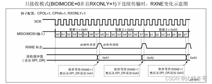
● One way receive only mode (BIDIMODE=0 also RXONLY=1)
─ SPE=1 when , Transmission begins ;
─ Only the receiver is activated , stay MISO Data received on pin , Sequentially shifted into 8 Bit shift register , It is then transmitted in parallel to SPI_DR register ( Receive buffer ) in .
● Two way mode , When sending (BIDIMODE=1 also BIDIOE=1)
─ When writing data to SPI_DR register ( Transmit buffer ) after , Transmission begins ;
─ While transmitting the first bit of data , Data is transferred in parallel from the transmit buffer to 8 Bit shift register , It is then serially shifted to MOSI On the pin ;
─ Do not receive data .
● Two way mode , Reception time (BIDIMODE=1 also BIDIOE=0)
─ SPE=1 also BIDIOE=0 when , Transmission begins ;
─ stay MOSI Data received on pin , Sequentially shifted into 8 Bit shift register , It is then transmitted in parallel to SPI_DR register ( Receive buffer ) in .
─ Do not activate the transmitter , No data is sent serially to MOSI On the pin .
Start transmission in mode
● Full duplex mode (BIDIMODE=0 also RXONLY=0)
─ When the clock signal is received from the device and the first data bit appears in its MOSI when , Data transfer starts , The subsequent data bits are sequentially moved into the shift register ;
─ meanwhile , When transmitting the first data bit , The data in the transmit buffer is transmitted to in parallel 8 Bit shift register , It is then sent serially to MISO On the pin . The software must be guaranteed to be in SPI The master device writes the data to be sent in the send register before starting data transmission .
● One way receive only mode (BIDIMODE=0 also RXONLY=1)
─ When the clock signal is received from the device and the first data bit appears in its MOSI when , Data transfer starts , Then the data bits are sequentially moved into the shift register ;
─ Do not start the transmitter , No data is transmitted serially to MISO On the pin .
● Two way mode , When sending (BIDIMODE=1 also BIDIOE=1)
─ When the clock signal is received from the device and the first data bit in the transmission buffer is transmitted to MISO On the pin , Data transfer starts ;
─ The first data bit is transferred to MISO On the pin at the same time , The data to be transmitted in the transmission buffer is transmitted to in parallel 8 Bit shift register , It is then sent serially to MISO On the pin . The software must be guaranteed to be in SPI The master device writes the data to be sent in the send register before starting data transmission ;
─ Do not receive data .
● Two way mode , Reception time (BIDIMODE=1 also BIDIOE=0)
─ When the clock signal is received from the device and the first data bit appears in its MOSI when , Data transfer starts ;
─ from MISO The data received on the pin is transmitted serially to 8 Bit shift register , It is then transmitted in parallel to SPI_DR register ( Receive buffer ); ─ Do not start the transmitter , No data is transmitted serially MISO On the pin .
Process the sending and receiving of data
When data is transferred from the transmit buffer to the shift register , Set up TXE sign ( Send buffer empty ), It means that the internal transmit buffer can receive the next data ; If in SPI_CR2 Register is set TXEIE position , An interrupt is generated ; write in SPI_DR Register can be cleared TXE position .
notes : Before writing to the transmit buffer , The software must confirm TXE Mark is ’1’, Otherwise, the new data will overwrite the data already in the transmission buffer .
At the last edge of the sampling clock , When data is transferred from the shift register to the receive buffer , Set up RXNE sign ( The receive buffer is not empty ); It indicates that the data is ready , It can be downloaded from SPI_DR Register readout ; If in SPI_CR2 Register is set RXNEIE position , An interrupt is generated ; read out SPI_DR Register can be cleared RXNIE Sign a . In some configurations , When transmitting the last data , have access to BSY Flag waiting for the end of data transmission .
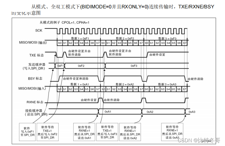
In master or slave mode (BIDIMODE=0 also RXONLY=0) Full duplex transmit and receive process mode
The software must follow the following process , Send and receive data :
- Set up SPE Position as ’1’, Can make SPI modular ;
- stay SPI_DR Write the first data to be sent in the register , This operation will clear TXE sign ;
- wait for TXE=1, Then write the second data to be sent . wait for RXNE=1, Then read out SPI_DR Register and get the first received data , read SPI_DR While clearing RXNE position . Repeat these operations , Send subsequent data and receive n-1 Data ;
- wait for RXNE=1, Then receive the last data ;
- wait for TXE=1, stay BSY=0 Then close SPI modular .
You can also respond RXNE or TXE This process is implemented in the handler of the interrupt generated by the rising edge of the flag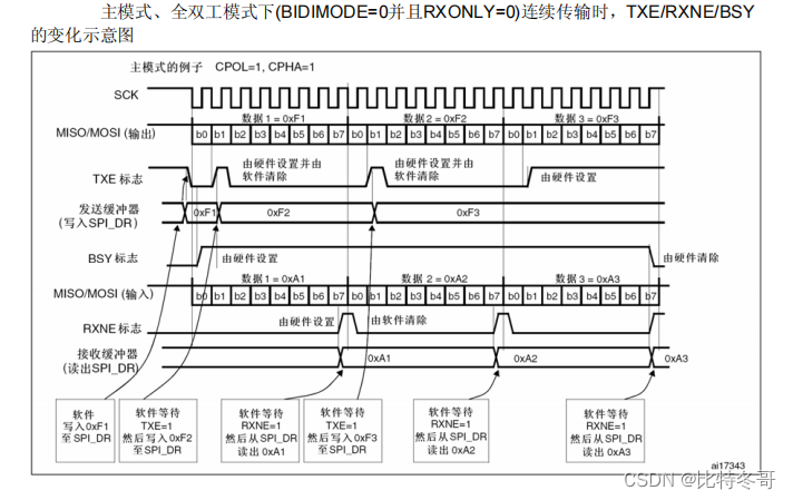
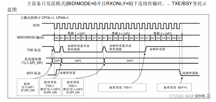
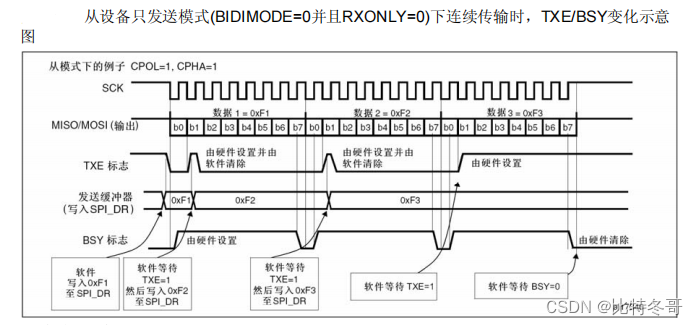
Only send the process (BIDIMODE=0 also RXONLY=0)
In this mode , The transmission process can be briefly described as follows , Use BSY Bit waits for the end of transmission : - Set up SPE Position as ’1’, Can make SPI modular ;
- stay SPI_DR Write the first data to be sent in the register , This operation will clear TXE sign ;
- wait for TXE=1, Then write the second data to be sent . Repeat this operation , Send subsequent data ;
- Write the last data to SPI_DR After register , wait for TXE=1; And then wait BSY=0, This indicates that the transmission of the last data has been completed . You can also respond TXE This process is implemented in the handler of the interrupt generated by the rising edge of the flag .
notes :
- For discontinuous transmission , In the writing SPI_DR Operation and setting of registers BSY There is 2 individual APB Delay of clock cycle
late , So in send only mode , After writing the last data , Better wait first TXE=1, Then wait BSY=0. - In send only mode , In the transport 2 After data , Because the received data will not be read ,SPI_SR In register OVR The bit will change to ’1’.( Translation notes : Software doesn't have to care about this OVR Sign a )
Two way sending process (BIDIMODE=1 also BIDIOE=1)
In this mode , The operation process is similar to the send only mode , The difference is : In enabling SPI Module before , Need to be in SPI_CR2 Set BIDIMODE and BIDIOE Position as ’1’.
One way receive only mode (BIDIMODE=0 also RXONLY=1)
In this mode , The transmission process can be briefly described as follows ( see ):
- stay SPI_CR2 In the register , Set up RXONLY=1;
- Set up SPE=1, Can make SPI modular :
a) In main mode , Produce immediately SCK Clock signal , Closing SPI(SPE=0) Before , Continuously receive serial data ;
b) From mode , When SPI Pull down the main equipment NSS Signal and generate SCK Clock hour , Receive serial data . - wait for RXNE=1, Then read out SPI_DR Register to get the received data ( At the same time, it will clear RXNE position ). Repeat this operation to receive all data . You can also respond RXNE This process is implemented in the handler of the interrupt generated by the rising edge of the flag .
notes : If it is closed after the last data transmission SPI modular , Please follow the 23.3.8 Section .
One way receiving process (BIDIMODE=1 also BIDIOE=0)
In this mode , The operation process is similar to the receive only mode , The difference is : In enabling SPI Module before , Need to be in SPI_CR2 Set... In the register BIDIMODE by ’1’ And get rid of BIDIOE Position as ’0’.
Continuous and discontinuous transmission
When sending data in main mode , If the software is fast enough , Can detect every TXE The rising edge of ( or TXE interrupt ), And write immediately before the end of the ongoing transfer SPI_DR register , Can realize continuous communication ; here , Between the transmission of each data item SPI The clock remains continuous , meanwhile BSY Bits will not be cleared .
If the software is not fast enough , Will result in discontinuous communication ; At this time , It will be cleared between each data transmission ( See the picture below ). In the receive only mode of the main mode (RXONLY=1), Communication is always continuous , and BSY The flag is always ’1’. In slave mode , The continuity of communication is determined by SPI The main equipment decides . No matter what , Even if the communication is continuous ,BSY There will be at least one flag between each data item SPI The clock cycle is low 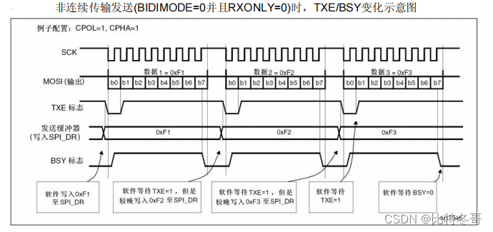
6. CRC Calculation
CRC Verification is used to ensure the reliability of full duplex communication . Data transmission and data reception use separate CRC Calculator . It is calculated by programmable polynomial operation on each receiving bit CRC.CRC Is calculated by SPI_CR1 In the register CPHA and CPOL Bit defined by the edge of the sampling clock .
Be careful : The SPI Interface provides two CRC computing method , Depends on the selected send and / Or received data frame format :8 Bit data frame adopts CR8;16 Bit data frame adopts CRC16.
CRC Calculation is done by setting SPI_CR1 In register CRCEN Bit enabled . Set up CRCEN Reset at the same time CRC register (SPI_RXCRCR and SPI_TXCRCR). When setting SPI_CR1 Of CRCNEXT position ,SPI_TXCRCR The content of will be sent after the current byte is sent .
In the transport SPI_TXCRCR When , If the value received in the shift register is the same as SPI_RXCRCR The content of does not match , be SPI_SR The register of CRCERR The flag bit is set 1.
If in TX There is data in the buffer ,CRC The value of is transmitted only after the data byte transmission ends . In the transport CRC period ,CRC The calculator is off , The value of the register remains unchanged .
Be careful : Please refer to the product manual , To confirm this function ( Not all models have this function ).
SPI Communication can be used through the following steps CRC:
● Set up CPOL、CPHA、LSBFirst、BR、SSM、SSI and MSTR Value ;
● stay SPI_CRCPR Register input polynomial ;
● By setting SPI_CR1 register CRCEN Bit enable CRC Calculation , This operation will also clear the register SPI_RXCRCR and SPI_TXCRC;
● Set up SPI_CR1 The register of SPE Bit start SPI function ;
● Start and maintain communication , Until only the last byte or half word is left ;
● When writing the last byte or half word into the transmit buffer , Set up SPI_CR1 Of CRCNext position , Indicates that the hardware sends the last data , send out CRC The numerical . Sending CRC Value period , stop it CRC Calculation ;
● When the last byte or halfword is sent ,SPI send out CRC The number ,CRCNext Bit is cleared . Again , The received CRC And SPI_RXCRCR Value comparison , If the comparison does not match , Is set SPI_SR Upper CRCERR Sign a , When you set SPI_CR2 The register of ERRIE when , Then there is an interruption .
Be careful :
- When SPI When the module is in slave mode , Please note that enable the clock after it stabilizes CRC Calculation , Otherwise, you may get the wrong CRC The result of the calculation is . in fact , As long as it's set CRCEN position , As long as SCK There is an input clock on the pin , No matter SPE Bit status , It's all going on CRC The calculation of .
- When SPI When the clock frequency is high , User is sending CRC You must be careful when . stay CRC During transmission , Use CPU The time should be as little as possible ; In order to avoid receiving the last data and CRC An error occurred when , Sending CRC Function calls should be prohibited during . You have to send / Finish setting before receiving the last data CRCNEXT Bit operation .
- When SPI When the clock frequency is high , because CPU The operation of will affect SPI The bandwidth of the , The proposal USES DMA Mode to avoid SPI Reduced speed .
- When STM32F10xxx Configured as slave mode and used NSS Hardware mode ,NSS Pins should be in data transmission and CRC Keep low during transmission .
- When configuring SPI For slave mode and use CRC The function of , Even if NSS When the pin is high, it will still execute CRC The calculation of ( Translation notes : When NSS When the signal is high , If SCK There are sometimes clock pulses on the pin , be CRC The calculation will continue ). for example : When the master device communicates with multiple slave devices alternately , This will happen ( Translation notes : Try to avoid CRC Misoperation of ). Uncheck a slave device (NSS The signal is high ) Switch to selecting a new slave (NSS The signal is low ) When , In order to keep the master-slave device next time CRC Synchronization of calculation results , Both sides of the master and slave should be cleared CRC The number .
Follow the steps below to clear CRC The number :
- close SPI modular (SPE=0);
- eliminate CRCEN Position as ’0’;
- Set up CRCEN Position as ’1’;
- Can make SPI modular (SPE=1).
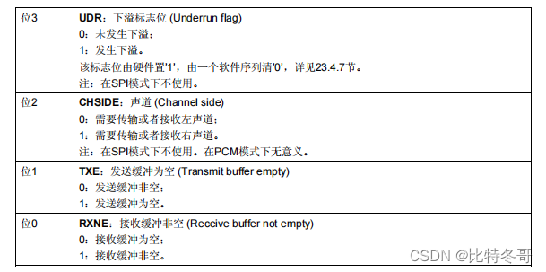
7. Status flag
Application through 3 A status flag can fully monitor SPI Status of the bus .
Send buffer free flag (TXE)
This flag is ’1’ Indicates that the transmit buffer is empty , You can write down a data to be sent and enter it into the buffer . When writing SPI_DR when ,TXE The flag is cleared .
The receive buffer is not empty (RXNE)
This flag is ’1’ Indicates that valid received data is contained in the receive buffer . read SPI The data register can clear this flag .
busy (Busy) sign
BSY The flag is set and cleared by hardware ( Writing this bit has no effect ), This flag indicates SPI Status of communication layer .
When it is set to ’1’ when , indicate SPI Busy communicating , With one exception : In the two-way receiving mode of the main mode (MSTR=1、BDM=1 also BDOE=0), During reception BSY The flag remains low . Before the software is shut down SPI Module and enter shutdown mode ( Or turn off the device clock ) Before , have access to BSY Flag to detect whether the transmission ends , This avoids destroying the last transmission , Therefore, it is necessary to strictly follow the following process .BSY Flags can also be used to avoid write conflicts in multi host systems .
In addition to the two-way reception mode of the main mode (MSTR=1、BDM=1 also BDOE=0), When the transmission starts ,BSY The sign is set ’1’.
This flag will be cleared to ’0’:
● When the transmission ends ( In main mode , Exception in case of continuous communication );
● When off SPI modular ;
● When the main mode failure occurs (MODF=1).
If the communication is not continuous , Then between the transmission of each data item ,BSY The flag is low .
When communication is continuous :
● In main mode : Throughout the transmission ,BSY Keep the sign high ;
● From mode : Between the transmission of each data item ,BSY Sign on a SPI Low in clock cycle .
notes : Do not use BSY The flag handles the sending and receiving of each data item , Best use TXE and RXNE sign .
8. close SPI
When the communication ends , Can be closed by SPI Module to terminate communication . eliminate SPE Bit to close SPI.
In some configurations , If retransmission is not complete , Just shut it down SPI Module and enter shutdown mode , The current transmission may be damaged , and BSY The logo has also become unreliable .
To avoid this , close SPI When the module , It is recommended to follow the following steps :
Full duplex mode in master or slave mode (BIDIMODE=0,RXONLY=0)
- wait for RXNE=1 And receive the last data ;
- wait for TXE=1;
- wait for BSY=0;
- close SPI(SPE=0), Finally, enter the shutdown mode ( Or turn off the clock of the module ).
One way send only mode in master or slave mode (BIDIMODE=0,RXONLY=0) Or two-way transmission mode (BIDIMODE=1,BIDIOE=1)
stay SPI_DR After the last data is written in the register :
- wait for TXE=1;
- wait for BSY=0;
- close SPI(SPE=0), Finally, enter the shutdown mode ( Or turn off the clock of the module ).
One way receive only mode in master or slave mode (MSTR=1,BIDIMODE=0,RXONLY=1) Or two-way receiving mode (MSTR=1,BIDIMODE=1,BIDIOE=0)
This situation requires special treatment , In order to make sure SPI Will not start a new transfer :
- Wait for the penultimate ( The first n-1 individual )RXNE=1;
- Closing SPI(SPE=0) Wait for one before SPI Clock cycle ( Use software delay );
- After entering the shutdown mode ( Or turn off the clock of the module ) Wait for the last one before RXNE=1.
notes : One way send only mode in main mode (MSTR=1,BDM=1,BDOE=0) when , During transmission BSY The flag is always low .
Receive only mode in slave mode (MSTR=0,BIDIMODE=0,RXONLY=1) Or two-way receiving mode (MSTR=0,BIDIMODE=1,BIDIOE=0)
- Can be closed at any time SPI(SPE=0),SPI It will be closed after the current transmission ends ;
- If you want to enter the shutdown mode , After entering the shutdown mode ( Or turn off the clock of the module ) You must wait before BSY=0.
9. utilize DMA Of SPI signal communication
To achieve maximum communication speed , Need to go to SPI Send buffer fill data , Similarly, the data in the receiving buffer must be read in time to prevent overflow . To facilitate high-speed data transmission ,SPI Implements a simple request / The answer is DMA Mechanism .
When SPI_CR2 When the corresponding enable bit on the register is set ,SPI The module can send DMA Transmission request . The transmit buffer and the receive buffer also have their own DMA request ( see ).
● When sending , In every time TXE Set to ’1’ Issued at DMA request ,DMA The controller writes data to SPI_DR register ,TXE The sign is therefore cleared .
● Reception time , In every time RXNE Set to ’1’ Issued at DMA request ,DMA The controller starts from SPI_DR Register reads data ,RXNE The sign is therefore cleared .
When using only SPI When sending data , Just enable SPI Sending of DMA passageway . here , Because the received data was not read ,OVR Be set to ’1’( Translation notes : The software doesn't have to pay attention to this sign ). When using only SPI When receiving data , Just enable SPI Reception DMA passageway .
In send mode , When DMA All data to be sent has been transmitted (DMA_ISR The register of TCIF The logo becomes ’1’) after , By monitoring BSY Mark to confirm SPI End of communication , This can avoid closing SPI Or when entering stop mode , Destroy the transmission of the last data . So the software needs to wait TXE=1, And then wait BSY=0.
notes : In discontinuous communication , Writing data to SPI_DR Operation and BSY Bit is set to ’1’ Between , Yes 2 individual APB Delay of clock cycle , therefore , Wait after writing the last data TXE=1 Wait for BSY=0.
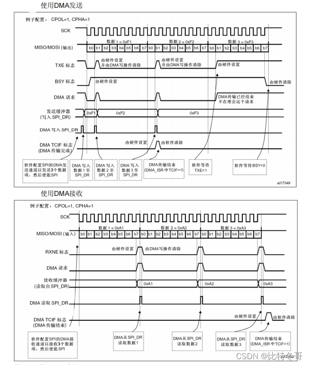
belt CRC Of DMA function
When enabled SPI Use CRC Verify and enable DMA Mode time , At the end of the communication ,CRC The sending and receiving of bytes are done automatically .
Data and CRC At the end of the transmission ,SPI_SR The register of CRCERR Mark is ’1’ Indicates that an error occurred during transmission .
10. Error flag
Main mode failure error (MODF)
Main mode failure occurs only in :NSS Pin hardware mode management , Of the main equipment NSS Feet pulled down ; Or in NSS Pin software mode management ,SSI Bit is set to ’0’ when ;MODF The bit is automatically set . Main mode failure pair SPI The equipment has the following effects :
● MODF Bit is set to ’1’, If set ERRIE position , Then SPI interrupt ;
● SPE The position is cleared as ’0’. This will stop all output , And close SPI Interface ;
● MSTR The position is cleared as ’0’, So force this device into slave mode .
The following steps are used to clear MODF position :
- When MODF Bit is set to ’1’ when , Carry out a check on SPI_SR Read or write operation of register ;
- Then write SPI_CR1 register .
There are more than one MCU In the system , In order to avoid the conflict of multiple slave devices , You must first raise the NSS foot , Right again MODF Reset bit . After clearing ,SPE and MSTR Bits can be restored to their original state . For safety reasons , When MODF Position as ’1’ when , Hardware does not allow setting SPE and MSTR position . Normally configured , From the device's MODF Bit cannot be set to ’1’. However , In multi master configuration , A device can be set up MODF In the case of bit , In slave mode ; here ,MODF Bit indicates that there may be a multi master conflict . The interrupt program can perform a reset or return to the default state to recover from the error state .
Overflow error
When the master device has sent data bytes , The slave device has not cleared the data generated by the previous data byte RXNE when , Overflow error . When an overflow error occurs :
● OVR Bit is set to ’1’; When you set ERRIE When a , Then there is an interruption .
here , The data in the receiver buffer is not new data sent by the master device , read SPI_DR The register returns previously unread data , All subsequent data is discarded .
Read out in turn SPI_DR Registers and SPI_SR The register can set OVR eliminate .
CRC error
When you set SPI_CR On the register CRCEN When a ,CRC The error flag is used to check the validity of the received data . If the value received in the shift register ( The sender sent SPI_TXCRCR The number ) With the receiver SPI_RXCRCR The values in the register do not match , be SPI_SR On the register CRCERR Set as a flag ’1’.
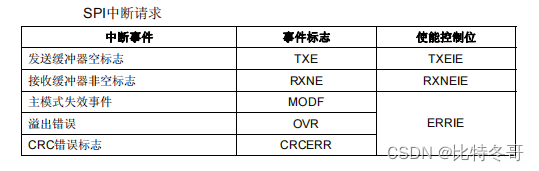
11. SPI interrupt
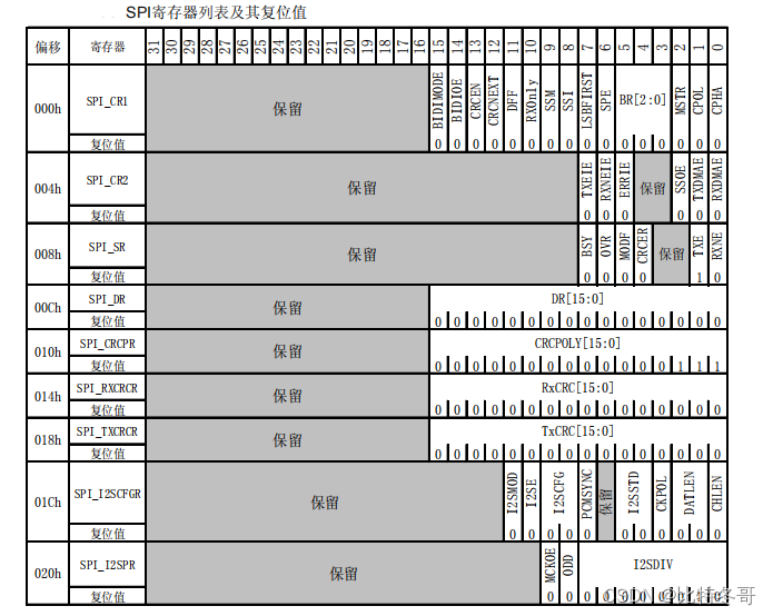
3、 ... and 、SPI Register description
1. SPI Control register 1(SPI_CR1)
2. SPI Control register 2(SPI_CR2)
3. SPI Status register (SPI_SR)
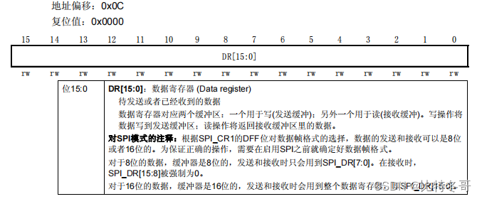
4. SPI Data register (SPI_DR)
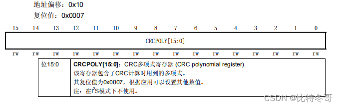
5. SPI CRC Polynomial register (SPI_CRCPR)
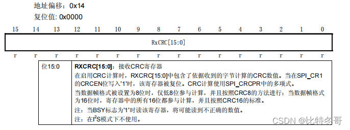
6. SPI Rx CRC register (SPI_RXCRCR)
7. SPI Tx CRC register (SPI_TXCRCR)
8. SPI_I2S Configuration register (SPI_I2S_CFGR)
9. SPI_I2S Prescaler register (SPI_I2SPR)
10. SPI Register address mapping
边栏推荐
- Appium foundation - use the first demo of appium
- [practical skills] how to do a good job in technical training?
- 1041 Be Unique
- 【云原生】微服务之Feign自定义配置的记录
- CF1634 F. Fibonacci Additions
- SQLMAP使用教程(一)
- leetcode-6108:解密消息
- Dynamic planning solution ideas and summary (30000 words)
- 【Rust 笔记】14-集合(下)
- Daily question 1342 Number of operations to change the number to 0
猜你喜欢
Typical use cases for knapsacks, queues, and stacks
LaMDA 不可能觉醒吗?
Dichotomy, discretization, etc
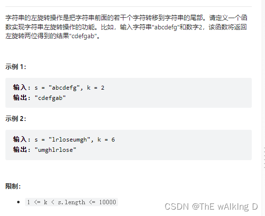
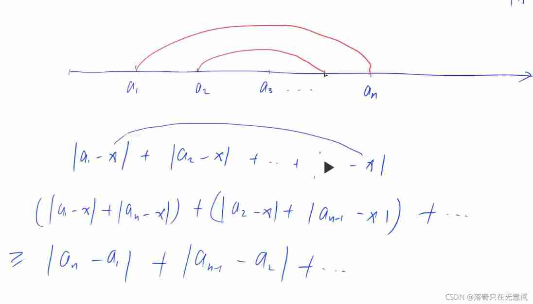
Sword finger offer 58 - ii Rotate string left
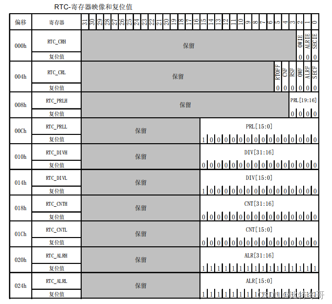
实时时钟 (RTC)
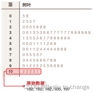
数据可视化图表总结(二)
liunx启动redis
1.14 - 流水线
SQLMAP使用教程(二)实战技巧一
Analysis of backdoor vulnerability in remote code execution penetration test / / phpstudy of national game title of national secondary vocational network security B module
随机推荐
MIT-6874-Deep Learning in the Life Sciences Week 7
开源存储这么香,为何我们还要坚持自研?
[rust notes] 14 set (Part 2)
Individual game 12
2017 USP Try-outs C. Coprimes
Cluster script of data warehouse project
Appium foundation - use the first demo of appium
MIT-6874-Deep Learning in the Life Sciences Week 7
个人开发的渗透测试工具Satania v1.2更新
Flutter Web 硬件键盘监听
1041 Be Unique
1.14 - 流水线
Appium automation test foundation - Summary of appium test environment construction
Binary search template
一些工具的记录2022
Data visualization chart summary (II)
【云原生】微服务之Feign自定义配置的记录
Spark中groupByKey() 和 reduceByKey() 和combineByKey()
Codeforces Round #732 (Div. 2) D. AquaMoon and Chess
leetcode-6108:解密消息