当前位置:网站首页>Design of KTV intelligent dimming system based on MCU
Design of KTV intelligent dimming system based on MCU
2022-07-05 02:31:00 【Salted fish brother】
word The full version can be downloaded as follows >>>>>>>>
Objective record
Abstract -------------------------------------------------------------- I
ABSTRACT--------------------------------------------------------- II
1 The introduction ----------------------------------------------------------- 1
1.1 Research background ----------------------------------------------- 1
1.2 Development trend ------------------------------------------------ 1
1.3 Design ideas and functions ------------------------------------------ 2
1.4 This chapter introduces -------------------------------------------- 2
2 Introduction to related chips --------------------------------------------------- 3
2.1 NE5532 amplifier ------------------------------------------- 3
2.2 AT89S52 Single chip microcomputer ------------------------------------------ 4
2.3 ADC0809 A / D converter -------------------------------------- 7
2.4 L297 controller --------------------------------------------- 9
2.5 L298 controller -------------------------------------------- 11
3 System hardware design -------------------------------------------------- 14
3.1 How the circuit works ------------------------------------------- 14
3.2 NE5532 Amplification circuit ---------------------------------------- 14
3.3 ADC0809 A / D conversion circuit ----------------------------------- 16
3.4 Reset circuit ----------------------------------------------- 17
3.5 Crystal oscillator --------------------------------------------------- 17
3.6 Key circuit ----------------------------------------------- 18
3.7 Light control circuit ------------------------------------------- 18
3.8 Motor control circuit ------------------------------------------- 18
4 System software design -------------------------------------------------- 20
4.1 KEIL Introduce ---------------------------------------------- 20
4.2 Overall program design ------------------------------------------- 20
4.3 Program design of rotating lamp ----------------------------------------- 21
4.3 Lighting program design ----------------------------------------- 22
5 Simulation and debugging ---------------------------------------------------- 23
6 Summary and prospect ---------------------------------------------------- 27
6.1 summary --------------------------------------------------- 27
6.2 expectation --------------------------------------------------- 27
reference --------------------------------------------------------- 28
thank ------------------------------------------------------------- 30
appendix ------------------------------------------------------------- 31
As the economy is changing , Our life pressure has also greatly increased , and KTV It is one of the places where people can relax . It is common in the market KTV The lights inside are fixed . This system designs an acoustooptic controller with the linkage of light and sound , In our era of heavy pressure, it has brought us a double experience of vision and hearing , With the melody of music, the colorful light and shadow and the memories of life make us more comfortable and comfortable at that moment .
This article will go through AT89S52 The single chip microcomputer controls the on and off of the strobe light and the speed of the rotating light in real time . So that a sound can be controlled by microphone KTV The phenomenon of bright and dark interior lights . I will adjust the brightness of the lighting lamp by using the button in the way of gradual turning on .
This design will use the concept of intelligent light regulation , It is realized by single chip microcomputer KTV Music acoustooptic control system , The result is that the light changes in real time with the change of sound size . The music atmosphere is excellent , Enhance the sense of space substitution , For parties 、KTV、 Bars and other occasions .KTV The emergence of music acoustooptic control system makes people get a double experience of hearing and vision , Same as It also brings fun and relaxation to people's tense and stressful life .
key word : Single chip microcomputer Dimming Voice control
ABSTRACT
As the economy changes with the times, the pressure of our life is greatly increased, and KTV is one of the places where people can relax. The lights in KTV, which is popular in the market, are all fixed. This system is designed as an acousto-optic controller with light and sound linkage, which brings us double experience of vision and hearing in our time of heavy pressure. With the melody of music, colorful light and shadow and memories of life, we can enjoy the comfort and coziness of that moment more.
In this paper, AT89S52 single chip microcomputer will be used to control the turning on and off of strongpoint and the speed of rotating lamp in real time. Thereby achieving the phenomenon that a sound controls the brightness and darkness of the lights in KTV through a microphone. And I will use the gradient lighting mode to make brightness level through buttons.
This design will use the concept of intelligent lighting adjustment, and realize the sound and light control system of KTV through single chip microcomputer. As a result, the lights will change in real time with the change of sound size. The music atmosphere is excellent, which enhances the sense of space substitution and is suitable for parties, KTV, bars and other occasions. The appearance of KTV's music sound and light control system gives people both auditory and visual experience, and also brings fun and relaxation to people's tense and stressful life.
Keywords:single-chip computer aiming sound-controlled
1 The introduction
1.1 Research background
Colorful lights have high quality 、 Low cost 、 Long life 、 The advantage of bright and soft lighting ,.......
Music acoustooptic control system is applicable to all music styles , It is applicable to both cheerful and passionate songs and sentimental songs . Professional lantern equipment has complex equipment operation , The price is expensive and the programming needs to be advanced .......
1.2 Development trend
With the rapid development of microcomputer software and hardware , Music acoustooptic control system and its interleaved application are more and more frequent , Music acoustooptic control system has become more and more complex 、 perfect . therefore , The microcomputer is used as the control part of the music acoustooptic control system .......
At present , The technology of music acoustooptic control system in China has gradually become mature , And towards intellectualization 、 Portability, compactness and diversification are developing rapidly . However , For some KTV The exploration of bars and so on is relatively ......
1.3 Design ideas and functions
First of all, the electret condenser microphone receives weak external analog signals , After rectification, filtering and amplification by the detection circuit and the amplification circuit , Re pass A/D The analog-to-digital converter is converted into a digital signal , Finally send it to AT89S52 Single chip computer to ......
1.4 This chapter introduces
Chapter one : It mainly introduces the research background, development trend and design ......
Chapter two : This paper mainly introduces what can be used in the acoustooptic control system ......
The third chapter : Mainly introduces the working principle of the circuit ......
Chapter four : Mainly introduce each software module ......
The fifth chapter : Mainly introduces simulation and debugging ......
Chapter six : It mainly introduces the summary and Exhibition .....
2 Introduction to related chips
2.1 NE5532 amplifier
(1) Chip introduction
NE5532 The voltage ratio of is relatively wide , Its voltage adaptation range is from ±3V To ±20V. Even now, it is recognized as the most cost-effective and practical operational amplifier .NE5532 With high performance and ultra-low noise 、.......
(2) The main features
Small signal bandwidth : 10MHZ
Output drive capability : 600Ω,10V Valid values
.......
(3) Pin description
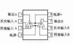
chart 2-1 NE5532 8 Pin diagram
1 foot : The output of the first amplifier
2 foot : The inverting input of the first amplifier
3 foot : In phase input of the first amplifier
......
2.2 AT89S52 Single chip microcomputer
(1) Chip introduction
AT89S52 MCU is a complementary metal oxide semiconductor with high performance and low power consumption 8 Bit MCU ......
AT89S52 SCM has the following standard functions :
8K Program memory .
......
(2) The main features
And MCS—51 SCM products are compatible .
Yes 8K Byte programmed flash memory .
......
(3) Pin description
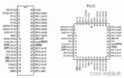
chart 2-2 AT89S52 Pin figure
The following table 2-1 by AT89S52 Of P0 And P3 Introduction to ports .
surface 2-1 AT89S52 Port Introduction
P0-P3 | Pin Introduction |
P0 mouth :P0.0-P0.7 39-32 foot | Bidirectional input and output port , Address external program memory as bidirectional 8 Bit data port and output are low 8 Bit address multiplexing port ; It can be used as 8 The level bidirectional input and output port is used .P0 A pull-up FET is designed inside the mouth . |
P1 mouth :P1.0-P1.7 1-8 foot | Quasi bidirectional input and output port , When output, everything is normal , If it is used as an input port, a high level should be given outside it .P1 A pull-up resistor is designed inside the port . |
P2 mouth :P2.0-P2.7 21-28 foot | Bidirectional input and output port , High output when addressing external program memory 8 Bit address ; It can be used as 8 The level bidirectional input and output port is used .P2 A pull-up resistor is also designed inside the mouth . |
P3 mouth :P3.0-P3.7 10-17 foot | Dual function bidirectional input and output port , Can receive output 4 individual TTL Gate current . When P3 After a high level at the port , They are internally pulled up to high level , And used as input .P3 A pull-up resistor is designed inside the port ,P3 The mouth also has a second function |
9 Pin RST: Reset end .
18 Pin XTAL2: On chip oscillation circuit output .
......
P1 The port has a second function , As shown in the table 2-2 Shown .
surface 2-2 AT89S52 Of P1 Introduction to the second function of port
P1 Port pin number | Second function |
P1.0 T2 | ( Timer / Counter T2 External count input of ), Clock output |
P1.1 T2EX | ( Timer / Counter T2 The capture of / Heavy load trigger signal and direction control ) |
P1.5 MOSI | Used in system programming |
P1.6 MISO | Used in system programming |
P1.7 SCK | Used in system programming |
P1 Port and port P3 Ports have their second function , Here are P3 The second function of the port , As shown in the table 2-3 Shown .
surface 2-3 AT89S52 Of P3 Introduction to the second function of port
P3 mouth | Second function |
P3.0 | RXD( Serial input port ) |
P3.1 | TXD( Serial output port ) |
P3.2 | INTO( External interruption 0) |
P3.3 | INT1( External interruption 1) |
P3.4 | TO( timing / Counter 0) |
P3.5 | T1( timing / Counter 1) |
P3.6 | WR( External data Memory write strobe ) |
P3.7 | RD( External data Memory read strobe ) |
2.3 ADC0809 A / D converter
(1) Chip introduction
ADC0809 yes CMOS Monolithic successive approximation A/D converter , It consists of 8 Analog switch 、 Address latch and decoder 、 The comparator 、8 Position switch tree A/D converter 、 Successive approximation register 、.....
(2) The main features
8 Bit resolution .
With controllable tristate output buffer .
......
(3) Pin description
Here are ADC0809 Pin figure , Pictured 2-3 Shown .
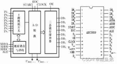
chart 2-3 ADC0809 Pin figure
Here are ADC0809 Detailed introduction of each pin , As shown in the table 2-4 Shown .
surface 2-4 ADC0809 Pin Introduction
ADC0809 Pin | Pin introduction |
(1)IN0~IN7 | 8 Way analog input , adopt 3 Root address decoding line ADDA、ADDB、ADDC Choose the passage . |
(2)D7~D0 One A/D | The converted data output end , Three state controllable output , Therefore, it can be directly connected with the microprocessor data line .8 The order of bits is D7 Is the highest position ,DO It's the lowest point . |
(3)ADD.AADDB.ADDC | Analog channel selection address signal ,ADDA It's low ,ADDC High position . |
ADC0809 Pin | Pin introduction |
(4)VR(+).VR(-) | just 、 Negative reference voltage input , Used to provide on-chip DAC Reference voltage of resistance network . In case of unipolar input ,VR(+)=5V, VR(-)=0V; When bipolar input ,VR(+)、 VR(-) Correct them respectively 、 Negative reference voltage . |
(5) ALE | Address latch allow signal , High active . When this signal is valid ,A、B、C The three bit address signal is latched , Decode and gate the corresponding analog channel . When use , This signal is often associated with START The signal is connected - rise , To lock the channel address and start at the same time A/D transformation . |
(6) START—A/D | Switching start signal , The positive pulse works . The rising edge of the pulse applied to this end clears the successive approximation register , The falling edge begins A/D transformation . If a new start pulse is received while switching , The original conversion process is aborted , Start the conversion again . |
(7) E0C | Conversion end signal , High active . The signal is in A/D Low level during conversion , The rest of the time is high . This signal can be used as CPU Status signal of query , It can also be used as a pair CPU Interrupt request signal of . When it is necessary to continuously sample a certain analog quantity 、 In the case of conversion ,EOC It can also be fed back to as a starting signal START End , However, it needs to be started by the external circuit for the first time when it is just powered on . |
(8) 0E | Output permissive signal , High active . When the microprocessor sends this signal ,ADC0808/0809 The output tristate gate of is opened , Make the conversion result read through the data bus . In interrupted working mode , The signal is often CPU Interrupt request response signal sent . |
2.4 L297 controller
1、 Chip introduction
L297 It is a special controller for stepping motor , It can produce 4 Phase control signal , It can be used for computer-controlled two-phase bipolar and four phase single-phase stepping motors , Can use single four beats 、 Double four beat 、 Four phases and eight beats Control stepping electricity ......
2、 The main features
L297 Its feature is that it only needs a clock 、 Direction and mode input signals . The phase is generated internally , Therefore, it can reduce the burden of MCU and program design .
(1) Reset input and home output
(2) A few external components
......
3、 Pin description
chart 2-4 L297 Pin figure
1 foot (SYNC)—— Chopper output . If more than one 297 Synchronous control , be-all SYNC The ends must be connected together , Share a set of oscillation elements . If an external clock source is used , Then the clock signal is connected to this pin .
2 foot (GND)—— Ground terminal .
3 foot .......
2.5 L298 controller
1、 Chip introduction
L298 Is to use 15 Lead wire Multiwatt and PowerSO20 Packaged integrated monolithic circuit . It is a high voltage , High current double full bridge driver , Designed to accept Standards TTL Logic level and drive inductive load , For example, relays , Solenoid ,DC And stepping motor . Not only two enable inputs are provided ......
2、 The main features
(1)TTL control input .
(2) Overheating protection .
......
3、 Pin Introduction
chart 2-5 L298 Pin figure
1 Foot current sensing A A detection resistance is connected between the pin and the ground , To control the load current .
2 Foot output 1,3 Foot output 2 H Bridge A Output . The current flowing through the load between these two pins is at pin 1 Monitoring at .
.......
3 System hardware design
3.1 How the circuit works
This design first uses electret condenser microphone to pick up the external audio signal . Then, the picked up weak external analog signal is filtered and amplified before passing A/D Analog to digital converter converts into digital signal ,......
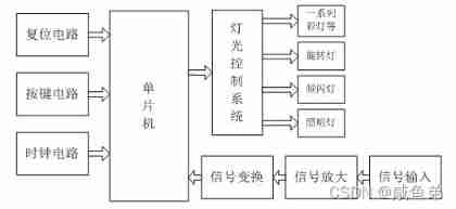
chart 3-1 Overall system framework diagram
3.2 NE5532 Amplification circuit
First, a weak AC analog signal is transmitted from the front end of a microphone , Through a diode peak detector, all AC analog signals in the clutter can be rectified and turned into smooth DC analog signals ,.....
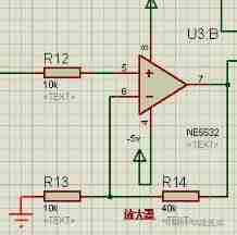
chart 3-2 NE5532 Amplification circuit
NE5532 It is a high-performance low-noise dual operational amplifier integrated circuit . Similar to many standard operational amplifiers , But it has better noise performance , Excellent output driving ability and quite high small signal bandwidth , Features such as large power supply voltage range ........
surface 3-1 NE5532 Limit rating
Parameters | Symbol | NE5532 | Company . |
Supply voltage | Vcc | ±22 | V |
Differential input voltage | Vdif | ±0.5 | V |
Input voltage | Vi | Supply voltage | V |
Power waste ,Tamb=25C | PD | 1100 | mW |
working temperature | TOPR | 0~70 | ℃ |
Here are NE5532 Basic electrical characteristics of , As shown in the table 2-3 Shown .
surface 3-2 NE5532 Electrical characteristics
Parameters | Symbol | Testing conditions | minimum value | standard | Maximum | Company |
Input offset voltage | Vos | 0.5 | 4 | mV | ||
Input offset current | Ios | 10 | 150 | nA | ||
Input bias current | IB | 200 | 800 | nA | ||
Supply current | Icc | 6 | 16 | mA | ||
Parameters | Symbol | Testing conditions | minimum value | standard | Maximum | Company |
Common mode input range | Vcm | ±12 | ±13 | V | ||
Common mode rejection ratio | CMRR | TA=25℃ | 70 | 100 | dB | |
Power rejection ratio | PSRR | TA=25℃ | 10 | uV/V | ||
Output voltage range | VO(P-P) | RL≥600Ω | ±12 | ±13 | ||
Input resistance | RI | TA=25℃ | 30 | 300 | kΩ | |
Short circuit current | ISC | 38 | mA | |||
Overshoot | OS | RL=600Ω CL=100PF | 10 | 20 | % | |
Voltage gain | GV | f=10kHz | 2 | 2.2 | V/mv | |
Gain bandwidth | GBW | CL=100PF RL=600Ω | 8 | 10 | MHZ |
3.3 ADC0809 A / D conversion circuit
adopt NE5532 The operational amplifier converts into a relatively large analog signal after ADC0809 The analog-to-digital converter converts into a digital signal . Pictured 3-3 As shown in the for ADC00809 A / D conversion circuit .
chart 3-3 ADC0809 A / D conversion circuit
3.4 Reset circuit
There are two ways to reset , One is automatic reset after power on , The second is manual reset , After reset, the MCU returns to the register 00 Address , Reset generally requires the pull-up resistor on the upper section and the reset switch . This design uses power on automatic reset and manual reset ,...... Pictured 3-4 Shown .
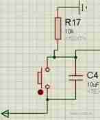
chart 3-4 Reset circuit
3.5 Crystal oscillator
AT89S52 There are usually two basic ways to control the internal clock control signal of single chip microcomputer ,...... Pictured 3-5 Shown .
chart 3-5 Crystal oscillator circuit
3.6 Key circuit
Because the system needs to realize the lighting and other lights on and off , We use independent keys to achieve . We simulate a button to control the strobe light on and off , A group of lighting switches control the brightness adjustment and switch of the lighting lamp . One ......
3.7 Light control circuit
LED The color lamp control circuit is actually a color lamp 、 Rotating lights 、 Radium spotlight 、 Backlight 、 Soft light 、 Return light 、 Strobe light 、 A circuit composed of lamps and other parts . Pictured 3-6 Shown .KTV One of the commonly used lamps now is laser lamp , Now there is a private room laser lamp specially designed for private rooms , The feature is that it can be used continuously for a long time , To fill with ...... Pictured 3-6 Shown .
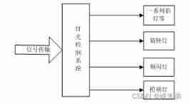
chart 3-6 Light control circuit frame diagram
3.8 Motor control circuit
L297 and L298n Combinational circuit module . Pictured 3-8 Shown . among L297 Generate four phase drive signal , ......
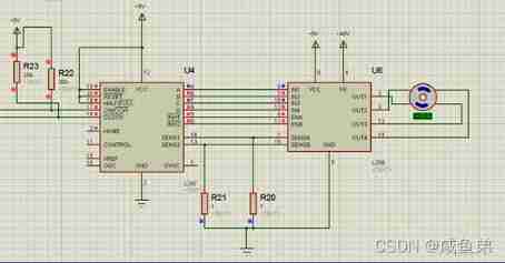
chart 3-7 Motor control circuit
4 System software design
4.1 keil Introduce
keilc51 Is based on the use of micro SCM c Language hardware programming software development of the general operating system , Comparison with other assembly languages ,c Language has obvious technical advantages in four basic functions ,......
4.2 Overall program design
First, the electret capacitor microphone receives the external weak analog signal, which is filtered and amplified before passing A/D Analog to digital converter converts into digital signal , Finally send it to AT89S52 The single chip microcomputer can control in real time LED The light-emitting lamp is on .......
This control system is composed of two parts : One is analog circuit , The second is digital circuit . The analog circuit is divided into three parts , It is composed of electret condenser microphone and diode peak detection circuit and is responsible for amplification operation ....... chart 4-1 Is the overall flow chart .
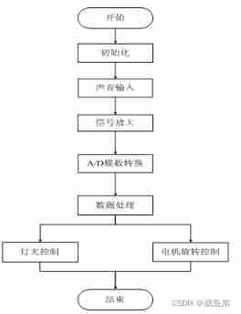
chart 4-1 Overall flow chart
4.3 Program design of rotating lamp
The rotary lamp has two control modes , Mode 1 automatic control , Through the size of the music to control the rotation speed of the rotating light in real time . Mode passive control , Press the key to control the speed of rotating light . By automatic / Manual switch button , Come on ...... Pictured 4-2 Shown .
chart 4-2 Rotating light control flow chart
4.3 Lighting program design
The lighting circuit realizes a gradual change process by long pressing the button to lighten and darken the light ,......
chart 4-3 Lighting flow chart
5 Simulation and debugging
The environment of this design is Proteus Realized under software simulation ,Proteus With schematic layout 、PCB Automatic or manual wiring 、SPICE Circuit simulation 、 Interactive circuit simulation 、 Simulation processor and its peripheral circuits ......
We should carefully check whether there is any missing wiring in the simulation diagram before the simulation ......
When music is input , Strobe lights will be on and off in real time with the size of the music . The rotating light will also rotate at different speeds with the size of the music . You can also manually control the rotary lamp by switching ...... chart 5-1 It is the overall system simulation diagram .
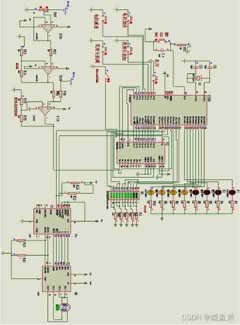
chart 5-1 Overall system simulation
(1) In the simulation, we can't clearly see the brightness of a lamp , So we use the number of lights in the simulation to represent the light off degree . Pictured 5-2 Shown .

chart 5-2 Strobe lamp simulation
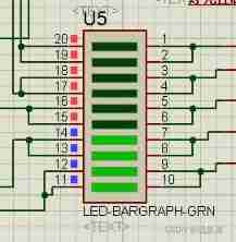
chart 5-3 Lighting simulation
The rotating light passes through a change-over switch . The music size can be realized to control the rotation speed and manually adjust the transformation from two modes . The slowest speed of rotating lamp is 0r/min, The fastest is 60r/min. actual 52r/min.

chart 5-4 Rotating lamp simulation
6 Summary and prospect
6.1 summary
In this paper, a design method based on AT89S52 Single chip microcomputer KTV Dimming system , The whole system is designed to make people have fun and relax in this tense and stressful life ........
In this graduation project , One of the main difficulties is the difficulty of using simulation software and keil uvision5 Strange programmer , Through serious study and actively consult with the students and teachers in school . I have gradually developed my own software ......
6.2 expectation
In the process of writing this graduation thesis and system design , Through continuous research and learning , Make me more connected to the knowledge of related chips . More familiar with protues Simulation software . The hardware circuit used in the simulation basically meets the system requirements . however , Due to the limited level of personal ability ,KTV Intelligent dimming system still has a lot of ......
You can download detailed information at the following link
边栏推荐
- From task Run get return value - getting return value from task Run
- GFS分布式文件系统
- When the low alcohol race track enters the reshuffle period, how can the new brand break the three major problems?
- 【LeetCode】106. Construct binary tree from middle order and post order traversal sequence (wrong question 2)
- Yuan universe also "real estate"? Multiple second-hand trading websites block metauniverse keywords
- Medusa installation and simple use
- 【LeetCode】501. Mode in binary search tree (2 wrong questions)
- Open source SPL optimized report application coping endlessly
- "C zero foundation introduction hundred knowledge and hundred cases" (72) multi wave entrustment -- Mom shouted for dinner
- Some query constructors in laravel (2)
猜你喜欢

Grub 2.12 will be released this year to continue to improve boot security
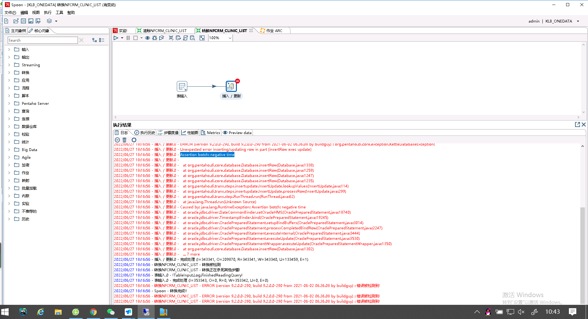
Spoon inserts and updates the Oracle database, and some prompts are inserted with errors. Assertion botch: negative time
Elfk deployment

. Net starts again happy 20th birthday

Practice of tdengine in TCL air conditioning energy management platform

Official announcement! The third cloud native programming challenge is officially launched!
Chinese natural language processing, medical, legal and other public data sets, sorting and sharing
R language uses logistic regression and afrima, ARIMA time series models to predict world population
Pytest (5) - assertion

Design and practice of kubernetes cluster and application monitoring scheme
随机推荐
Android advanced interview question record in 2022
Timescaledb 2.5.2 release, time series database based on PostgreSQL
Pgadmin 4 V6.5 release, PostgreSQL open source graphical management tool
Three properties that a good homomorphic encryption should satisfy
Video display and hiding of imitation tudou.com
Pytest (4) - test case execution sequence
Security level
Grub 2.12 will be released this year to continue to improve boot security
Character painting, I use characters to draw a Bing Dwen Dwen
d3js小记
Kotlin - 协程 Coroutine
Restful Fast Request 2022.2.1发布,支持cURL导入
openresty ngx_ Lua variable operation
Structure of ViewModel
When the low alcohol race track enters the reshuffle period, how can the new brand break the three major problems?
Use the difference between "Chmod a + X" and "Chmod 755" [closed] - difference between using "Chmod a + X" and "Chmod 755" [closed]
Bumblebee: build, deliver, and run ebpf programs smoothly like silk
Collection of gmat750 wrong questions
Hmi-30- [motion mode] the module on the right side of the instrument starts to write
Yolov5 model training and detection