当前位置:网站首页>Parade ps8625 | replace ps8625 | EDP to LVDS screen adapter or screen drive board
Parade ps8625 | replace ps8625 | EDP to LVDS screen adapter or screen drive board
2022-07-08 01:10:00 【qq1659747718】
Parade PS8625| replace PS8625|EDP turn LVDS Panel to panel wiring or panel drive board scheme
S8625 (DP to LVDS) Is a DisplayPort To LVDS Converter scheme chip , It can realize dual channels DP Input , Double link LVDS Output .
meanwhile PS8625 Is a display port to LVDS Converter design PC machine , utilize GPU And display port (DP) Or display port (eDP) Output and acceptance LVDS Display panel for input .
PS8625 At present, there is a shortage of supplies , And the product cost is low , Taiwan richda CS5211 Can replace Parade PS8625/Parade PS8622, It can be completely replaced and compatible in function and performance .
C5211 Compare Parade PS8625 Advantages and innovations
Support Displayport To LVDS Protocol converter for , yes CPU/GPU Key modules to the display , For computer motherboard driver LVDS The screen , widely
Applied to all-in-one machine 、 Advertising machine 、 Industrial computer and other markets , Innovation points :
1. adopt GPIO To select the default 16 set EDID, It is convenient for users to debug
2. Unique receiver design , It achieves low power consumption and high performance
3. Single power supply design can save BOM cost
4. programmable SSC It can reduce electromagnetic interference
CS5211 And PS8625 The parameters are compared as follows :

CS5211 Design EDP turn LVDS replace Parade PS8625|EDP turn LVDS The block diagram of the design structure of the screen transfer wiring or screen drive board scheme is as follows :

CS5211 Design EDP turn LVDS To replace Parade PS8625|EDP turn LVDS Panel to panel wiring or panel drive board scheme The design schematic diagram is as follows :

CS5211 Design EDP turn LVDS To replace PS8625 To design EDP turn LVDS Screen connection or EDP turn LVDS Schematic diagram of screen drive board +PCB The board diagram is as follows :


replace PS8625 Design EDP turn LVDS Screen connection or EDP turn LVDS The detailed scheme information of the screen driver board is shown in the attachment below :
replace PS8625 Scheme design data
边栏推荐
- Study notes of single chip microcomputer and embedded system
- Binder core API
- Semantic segmentation model base segmentation_ models_ Detailed introduction to pytorch
- 13.模型的保存和載入
- Get started quickly using the local testing tool postman
- 12.RNN应用于手写数字识别
- Serial port receives a packet of data
- 50MHz generation time
- 133. 克隆图
- 大二级分类产品页权重低,不收录怎么办?
猜你喜欢
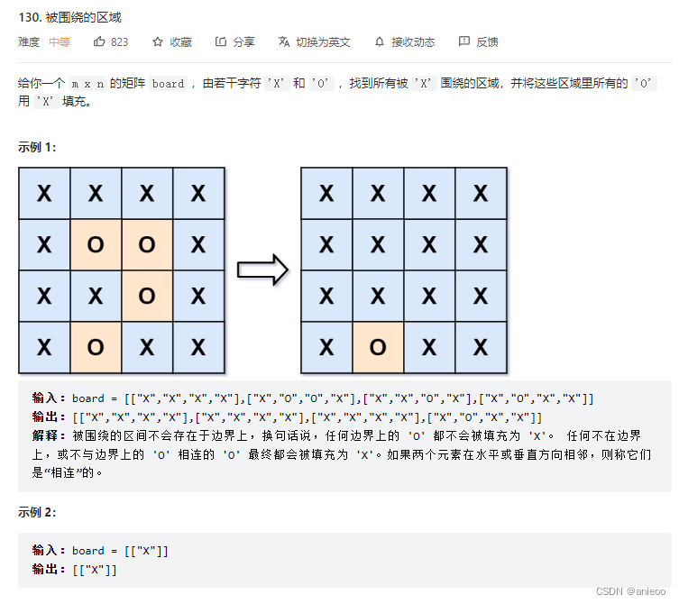
130. 被围绕的区域
13. Enregistrement et chargement des modèles
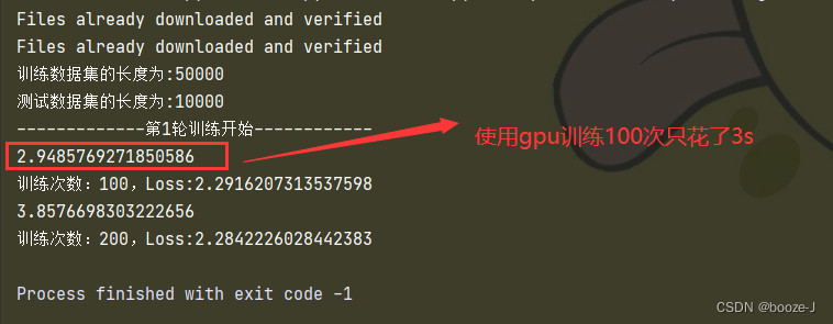
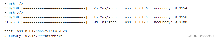
Using GPU to train network model
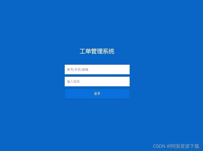
ThinkPHP kernel work order system source code commercial open source version multi user + multi customer service + SMS + email notification
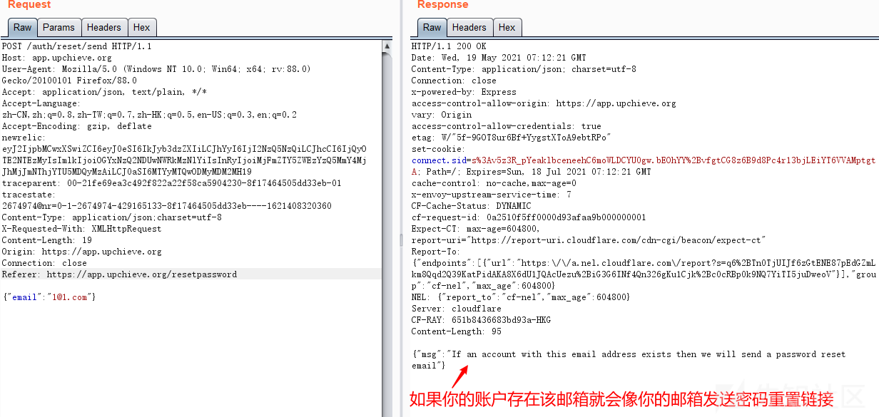
Password recovery vulnerability of foreign public testing
y59.第三章 Kubernetes从入门到精通 -- 持续集成与部署(三二)
SDNU_ ACM_ ICPC_ 2022_ Summer_ Practice(1~2)

How to write mark down on vscode
Several frequently used OCR document scanning tools | no watermark | avoid IQ tax
8.优化器
随机推荐
Su embedded training - Day6
C#中string用法
Su embedded training - Day5
Two methods for full screen adaptation of background pictures, background size: cover; Or (background size: 100% 100%;)
【深度学习】AI一键换天
Markdown learning (entry level)
How is it most convenient to open an account for stock speculation? Is it safe to open an account on your mobile phone
Chapter 7 Bayesian classifier
FOFA-攻防挑战记录
Introduction to paddle - using lenet to realize image classification method II in MNIST
ThinkPHP kernel work order system source code commercial open source version multi user + multi customer service + SMS + email notification
基于人脸识别实现课堂抬头率检测
完整的模型验证(测试,demo)套路
A speed Limited large file transmission tool for every major network disk
130. Zones environnantes
基于卷积神经网络的恶意软件检测方法
The whole life cycle of commodity design can be included in the scope of industrial Internet
Cve-2022-28346: Django SQL injection vulnerability
How does starfish OS enable the value of SFO in the fourth phase of SFO destruction?
国内首次,3位清华姚班本科生斩获STOC最佳学生论文奖