当前位置:网站首页>Blue Bridge Cup embedded (F103) -1 STM32 clock operation and led operation method
Blue Bridge Cup embedded (F103) -1 STM32 clock operation and led operation method
2022-07-08 01:18:00 【Youyu hesitant squid】
Blue Bridge Cup (F103)-1.STM32 Clock operation and LED Operation method
One 、STM32 Clock introduction
1. file location :
Open the resource packet → open 5- Competition board chip information → open STM32_CN.pdf
2. Introduction of clock tree (P56 Clock block diagram )
HSE OSC High speed external clock signal , In the Blue Bridge Cup F103rbt6 Develop on-board external crystal oscillator HSE=8MHz, Then a selector can choose 8MHz Or frequency division /2 by 4MHz, We choose 8MHz, Through the frequency multiplier , Frequency multiplier selection ×9 Make it work at the maximum output frequency 72MHz. Last pass AHB Prescaler output to peripheral .APB1 The maximum is 36MHz,APB2 The maximum is 72MHz.
3. Introduction of system structure (P25 System structure )
Mainly understand reset and clock control (RCC) Connect AHB The system bus , The bridge 1 by APB2, From the above ,APB2 For high frequency , The maximum clock frequency is 72MHz. The bridge 2 by APB1, For low frequency , The maximum clock frequency is 36Hz.
Mainly understand APB1( low speed ) and APB2( High speed ) Attached to APB equipment , Common peripherals are as follows :
APB1:I2C1,I2C2,UART4,UART5,SPI2,SPI3,RTC,TIM2~TIM7
APB2;ADC 1~3,USART1,SPI1,TIM1,TIM8,GPIO A ~ G,EXT1,AFIO
4. Turn on the peripheral clock with the library function
RCC_APB2PeriphClockCmd(RCC_APB2Periph_GPIOC,ENABLE);// Turn on GPIOC Peripheral clock
Two 、LED Operation method
1.LED initialization
Procedure steps :
LED initialization : Turn on the peripheral clock → Structure initialization → initialization GPIO
The code is as follows :
void LED_Init(void)
{

	GPIO_InitTypeDef GPIO_structure;// Declared structure
	RCC_APB2PeriphClockCmd(RCC_APB2Periph_GPIOC,ENABLE);/ Turn on the peripheral clock
	GPIO_structure.GPIO_Pin = GPIO_Pin_8|GPIO_Pin_9|GPIO_Pin_10|
	GPIO_Pin_11|GPIO_Pin_12|GPIO_Pin_13|GPIO_Pin_14|GPIO_Pin_15;// Initialization pin
	GPIO_structure.GPIO_Speed = GPIO_Speed_50MHz;// Initialize settings GPIO output frequency
	GPIO_structure.GPIO_Mode = GPIO_Mode_Out_PP;// Initialize settings GPIO Pattern
	GPIO_Init(GPIOC,&GPIO_structure);//GPIO initialization
}
2. Schematic diagram interpretation
(1)LED The circuit principle diagram 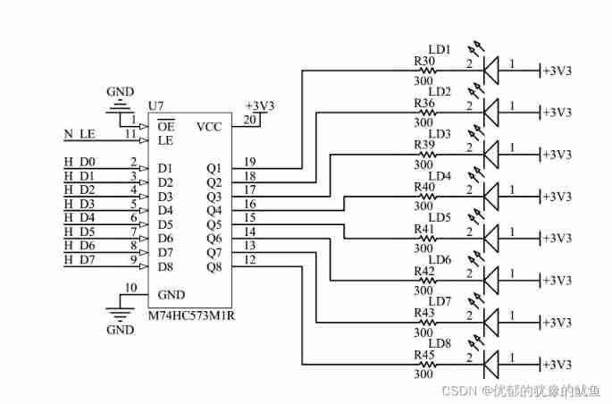
explain :LED Adopt common anode connection , Output low level is on LED.
Latch M74HC573: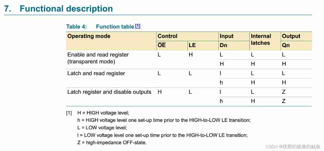
Function explanation :
According to the function description in the data book ,OE(Output Enable) Low power level , Output enable , In the circuit schematic diagram OE The terminal is directly grounded ,74HC573 Always in the enabled state .LE(Latch Enable) For high voltage ,D And Q Also for H or L.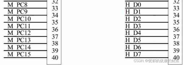

Be careful :
The left and right sides are connected through jumper caps , And STM32 Pin to pin
3. Realize the running water lamp
Procedure steps :
Running water lamp : Lighten up 1 individual LED→ Define an array → Use circulation to make LED Turn on .
The code is as follows :
void LED_contorl(void)
{

	u16 LED_ctrl;
	u8 LED_locate;
	u16 LED_code[8]={
    0x01,0x02,0x04,0x08,0x10,0x20,0x40,0x80};
	for(LED_locate=0;LED_locate<8;LED_locate++)
	{

		LED_ctrl=LED_code[LED_locate];
		GPIO_ResetBits(GPIOC,LED_ctrl<<8);
		Delay_Ms(500);
		GPIO_SetBits(GPIOC,LED_ctrl<<8);
	}
}
边栏推荐
- FIR filter of IQ signal after AD phase discrimination
- Ag9310 design USB type C to hdmi+u2+5v slow charging scheme design | ag9310 expansion dock scheme circuit | type-C dongle design data
- Four digit nixie tube display multi digit timing
- Using GPU to train network model
- Leetcode notes No.21
- Smart agricultural technology framework
- 13. Enregistrement et chargement des modèles
- Introduction to ML regression analysis of AI zhetianchuan
- 130. 被圍繞的區域
- Image data preprocessing
猜你喜欢
12.RNN应用于手写数字识别
A speed Limited large file transmission tool for every major network disk
9. Introduction to convolutional neural network

Invalid V-for traversal element style
![[necessary for R & D personnel] how to make your own dataset and display it.](/img/50/3d826186b563069fd8d433e8feefc4.png)
[necessary for R & D personnel] how to make your own dataset and display it.

5、离散控制与连续控制
Letcode43: string multiplication
Four digit nixie tube display multi digit timing
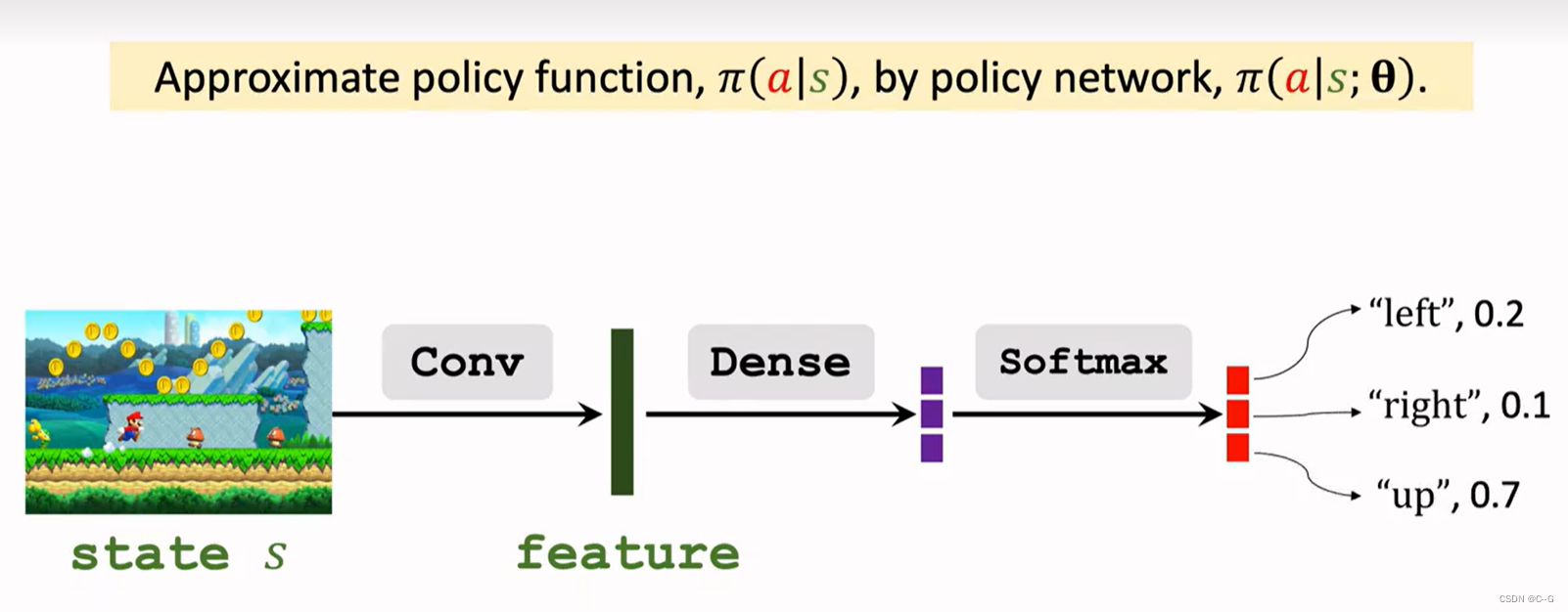
4、策略学习
USB type-C mobile phone projection scheme | USB type-C docking station scheme | TV / projector type-C converter scheme | ag9300ag9310ag9320
随机推荐
14. Draw network model structure
Markdown learning (entry level)
Basic realization of line graph
6. Dropout application
Capstone/cs5210 chip | cs5210 design scheme | cs5210 design data
The whole life cycle of commodity design can be included in the scope of industrial Internet
Chapter XI feature selection
3. MNIST dataset classification
3.MNIST数据集分类
Complete model training routine
13.模型的保存和載入
[go record] start go language from scratch -- make an oscilloscope with go language (I) go language foundation
Apt get error
Micro rabbit gets a field of API interface JSON
Ag7120 and ag7220 explain the driving scheme of HDMI signal extension amplifier | ag7120 and ag7220 design HDMI signal extension amplifier circuit reference
Smart grid overview
String usage in C #
Led serial communication
Su embedded training - Day6
Chapter improvement of clock -- multi-purpose signal modulation generation system based on ambient optical signal detection and custom signal rules